2006-2019 Microchip Technology Inc. DS30009711C-page 5
I/O Ports with PPS
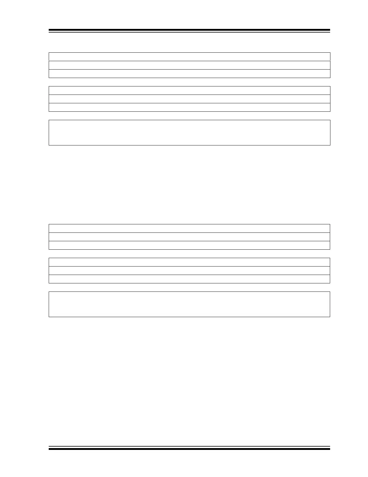
Register 2-1: TRISx: PORTx Data Direction Control Register
Register 2-2: PORTx: I/O Portx Register
R/W-1 R/W-1 R/W-1 R/W-1 R/W-1 R/W-1 R/W-1 R/W-1
TRISx<15:8>
(1)
bit 15 bit 8
R/W-1 R/W-1 R/W-1 R/W-1 R/W-1 R/W-1 R/W-1 R/W-1
TRISx<7:0>
(1)
bit 7 bit 0
Legend:
R = Readable bit W = Writable bit U = Unimplemented bit, read as ‘0’
-n = Value at POR ‘1’ = Bit is set ‘0’ = Bit is cleared x = Bit is unknown
bit 15-0 TRISx<15:0>: PORTx Data Direction Control bits
(1)
1 = The pin is an input
0 = The pin is an output
Note 1: Refer to the specific device data sheet for the actual implementation.
R/W-0 R/W-0 R/W-0 R/W-0 R/W-0 R/W-0 R/W-0
PORTx<15:8>
(1)
bit 15
R/W-0 R/W-0 R/W-0 R/W-0 R/W-0 R/W-0 R/W-0
PORTx<7:0>
(1)
bit 7
Legend:
R = Readable bit W = Writable bit U = Unimplemented bit, read as ‘0’
-n = Value at POR ‘1’ = Bit is set ‘0’ = Bit is cleared x = Bit is unknown
bit 15-0 PORTx<15:0>: I/O Portx bits
(1)
1 = The pin data are ‘1’
0 = The pin data are ‘0’
Note 1: Refer to the specific device data sheet for the actual implementation.