dsPIC33/PIC24 Family Reference Manual
DS30009711C-page 6 2006-2019 Microchip Technology Inc.
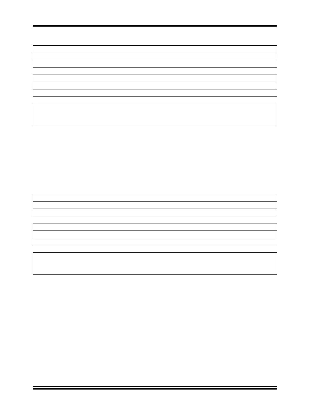
Register 2-3: LATx: PORTx Data Latch Register
Register 2-4: ODCx: PORTx Open-Drain Control Register
R/W-0 R/W-0 R/W-0 R/W-0 R/W-0 R/W-0 R/W-0 R/W-0
LATx<15:8>
(1)
bit 15 bit 8
R/W-0 R/W-0 R/W-0 R/W-0 R/W-0 R/W-0 R/W-0 R/W-0
LATx<7:0>
(1)
bit 7 bit 0
Legend:
R = Readable bit W = Writable bit U = Unimplemented bit, read as ‘0’
-n = Value at POR ‘1’ = Bit is set ‘0’ = Bit is cleared x = Bit is unknown
bit 15-0 LATx<15:0>: PORTx Data Latch bits
(1)
1 = The latch content is ‘1’
0 = The latch content is ‘0’
Note 1: Refer to the specific device data sheet for the actual implementation.
R/W-0 R/W-0 R/W-0 R/W-0 R/W-0 R/W-0 R/W-0 R/W-0
ODCx<15:8>
(1)
bit 15 bit 8
R/W-0 R/W-0 R/W-0 R/W-0 R/W-0 R/W-0 R/W-0 R/W-0
ODCx<7:0>
(1)
bit 7 bit 0
Legend:
R = Readable bit W = Writable bit U = Unimplemented bit, read as ‘0’
-n = Value at POR ‘1’ = Bit is set ‘0’ = Bit is cleared x = Bit is unknown
bit 15-0 ODCx<15:0>: PORTx Open-Drain Control bits
(1)
1 = The pin acts as an open-drain output pin if TRISx is ‘0’
0 = The pin acts as a normal pin
Note 1: Refer to the specific device data sheet for the actual implementation.