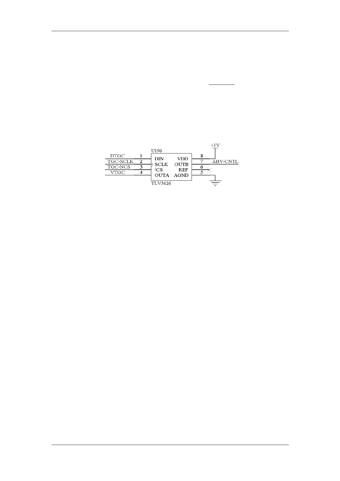
Overview
sending the analog voltage required by the voltage-controlled amplifier.
In practice, the internal 2.048V reference source is selected and after it is transformed
through TLV5626, the external output voltage is
. In theory, the
output range of its global transform is between 0V and 4.096V, which can meet the
requirements that the control voltage of ATGC is between 0V and 3V, as well as the
requirements that the adjustment signal of PHV is between 0V and 4V.
Figure 3-44 ATGC voltage generating circuit
6. Low-pass filter and stopping direct current circuit
The low-pass filter is used to provide the anti-aliasing filtering function for the ADC circuit.
The stopping direct current circuit is used for the direct-current component of the output
signal of the voltage-controlled gain amplifier circuit, enabling it to couple the direct
current level required by the ADC circuit before it enters the ADC.
7. A/D circuit
MAX1196 made by MAXIM is used as ADC. In practice, power is supplied respectively to
its analog and digital portions, and the analog portion is supplied with
+
3V and digital
portion with
+
3.3V.
The MAX1196 provides a dual-channel difference input ADC. The output port of the
digital signal after AD conversion is time-sharing multiplex, and the sampling rate is up to
40MHz and the resolution is 8 bits, which can meet the requirements of the system. In
addition, the range of the difference input signal is
V, which can also meet the
requirement of 2V
P-P
from the system.
2.1.1.4Beamforming
The amplified echo signal passes the ADC circuit to complete the analog-digital
3-8 DP-3300/DP-3200 Service Manual(V1.1)