Overview
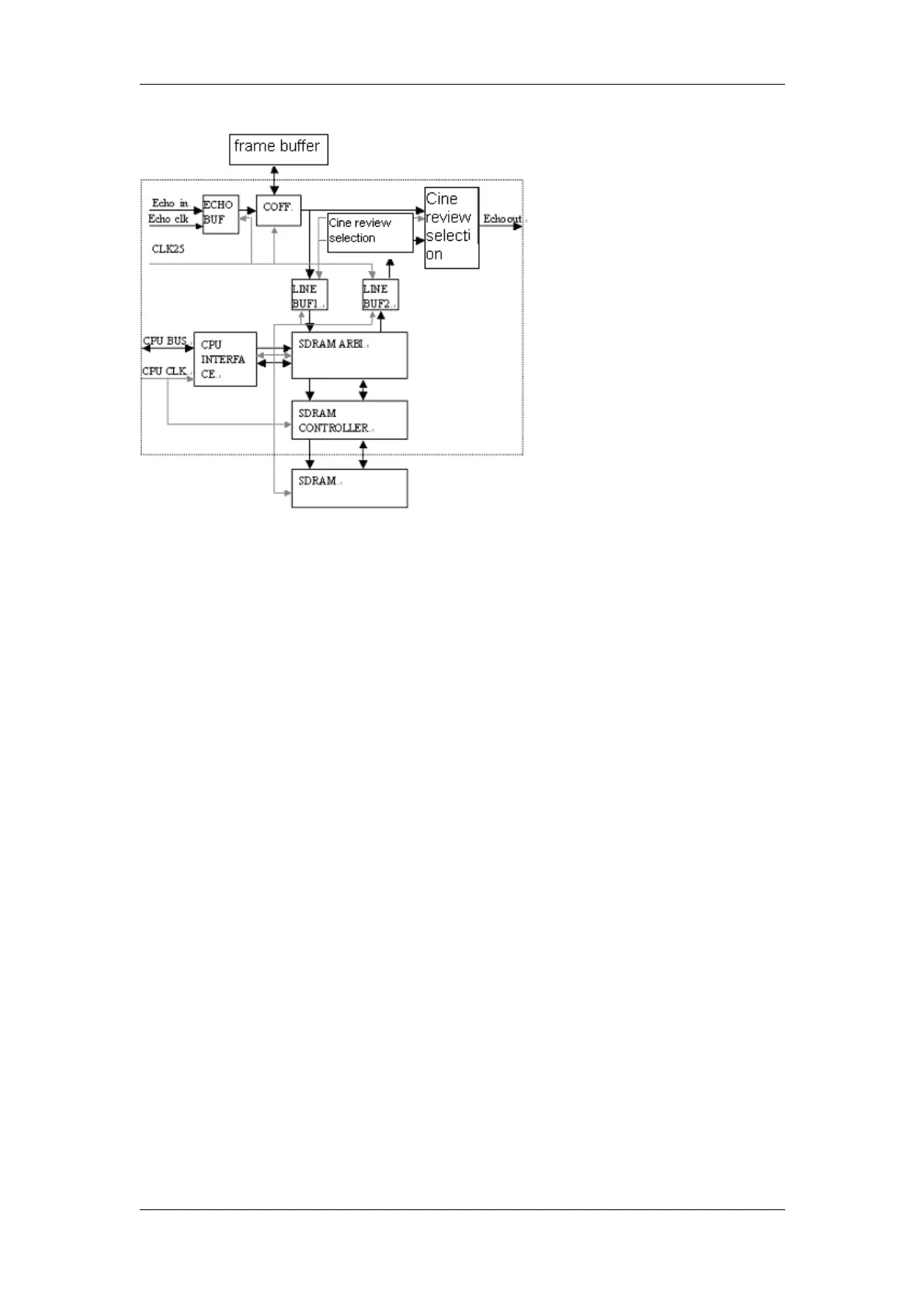
Figure 3-7 Schematic diagram of Cine review
The FPGA is mainly used to realize the control logic of the frame correlation circuit, and
the control logic of the Cine review memory. It is to note that this FPGA is also used for
the post-processing and display circuit.
The SRAM is used to realize the buffer function, and to provide the memory space of
128k*8 bits, and it can store one frame of high-density scanning line data. The frame
buffer always stores the most recent frame of the scanning line data which have gone
through frame correlation operation. The SDRAM is used to realize the memory function
of Cine review, and to provide the memory space of 4M*16 bits. One piece of SDRAM is
adopted to store 64-frame high-density images or 128-frame low-density images. The
control logic of the SDRAM is generated by the FPGA.
2.1.1.7DSC
The DSC is realized by means of one FPGA
(
ACEX1K100QC208-3
)
, four
W24L010A
(
B-mode DSC memory
)
, and one IS61LV25616L
(
B-mode scanning line
look-up table and M-mode DSC memory
)
. The M-MAX circuit is added before the M line
correlation circuit, and the M-mode memory only stores the 512-line images, so that the
M-mode memory and the B-mode DSC look-up table can share one 256K*16
SRAM
(
IS61LV25616L
)
. The M-MAX sampling circuit, M line correlation circuit, M-
mode DSC and B-mode DSC are realized through one FPGA
(
ACEX1K100QC208-3
)
.
3-10 DP-3300/DP-3200 Service Manual(V1.1)