143
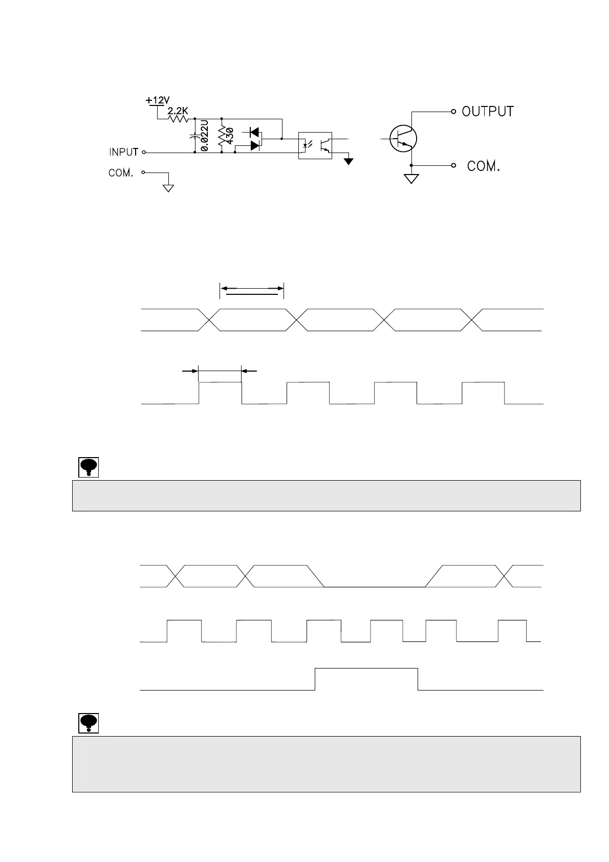
16-2-8. Equivalent circuit of input/output
16-2-9. Timing chart
(1) Normal
At the time of data output of each P.C., DATA and POL., output transistor will become ON (Negative
logic electrically).
(2) When the data is over
At the time of OVR output, output transistor will at the OVER signal will become ON (Negative logic
electrically). Moreover, for all of the DATA, output transistor will become OFF (Positive logic
electrically) at the time of OVER output. (However, for the POL., normal OFF at the [OL], and normal ON
at the [-OL]).
DATA
POL.
P.C.
OVER
ON
ON
ONONON ON ON
Input section
Output section
V
CE
=DC30 V
I
=DC20 mA MAX
3
3
DATA
POL.
P.C.
ON ON
ON
ON
ON
ON
ON ON
4 Times/s:Approx. 125 ms/ Approx. 25 ms/ Approx. 5 ms changeable
20 Times/s:Approx. 25 ms/ Approx. 5ms changeable
100 Times/s:Approx. 5 ms
4 Times/s:Approx. 250 ms
20 Times/s:Approx. 50 ms
100 Times/s:Approx. 10 ms
4 times/s : Approx. 250 ms
20 times/s : Approx. 50 ms
100 times/s : Approx. 10 ms
4 times/s : Approx. 125 ms / Approx. 25 ms / Approx. 5 ms changeable.
20 times/s : Approx. 25 ms / Approx. 5 ms changeable.
100 times/s : Approx. 5 ms
 Loading...