TRANSCEIVER 800 MHz MTP700 Portable Radio / Detailed Service Manual 4.2 - 17
Frequency Generating Section, Detailed Circuit Description
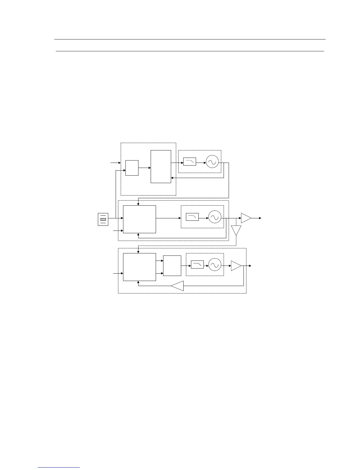
See Figure 4.2-8
This section describes the generating circuits that supply all the required frequencies for
the required transmitter and receiver functions. These circuits are described as follows:
• TCXO REF. Oscillator.
• Main VCO and Main Synthesizer.
• Second LO VCO and Dual Synthesizer RF section.
• Transmit PLL - TX VCO with the ESCORT Synthesizer IC.
Figure 4.2-8 Frequency Generation Section - Block Diagram
TCXO Reference Oscillator
The TCXO is the reference frequency source for all the radio synthesizers. The output of
the oscillator is a 16.8 MHz stable temperature compensated reference clock. This
oscillator’s centre frequency is adjustable by means of a PWM DAC (256 steps) to warp
the radio frequency in order to lock to the base station. This 16.8 MHz signal is present at
pin 3 of the TCXO, and is routed into the following devices:
1. To WPIC’s K6 XTALBASE pin. The signal is divided by 2 to produce the 8.4 MHz ref-
erence signal, which is used for the Main PLL synthesizer.
2. To LMX Dual Synthesizer’s OSC_IN pin via C731. The signal is divided to produce the
300 KHz reference signal for the second LO.
The reference signal is also routed from WPIC’s pin F10 (16.8_MHz_CLK) to GCAP3
(and subsequently to RedCap2) to clock the digital circuits.
219.3MHz
Reference
Oscillator - TCXO
RF Section
DOIF
FINIF2
Divider
300KHz
OSC_IN
Dual Synthesizer (U730)
SPIA-Bus
LPF
OSC
Second LO
To RX Mixer
915.65 – 979.65 MHz
Buffer
LPF
OSC
TX VCO
FREQA
IUP
ESCORT
FREQB
Buffer
To TX-LO Line-up
806 – 870 MHz
TX Synthesizer
SPIA-Bus IDOWN
I/V-
CONVERTER
36/32
LPF
OSC
Main VCOLOIN
XTALBASE CPGITR
WPIC
PRSCIN
To ESCORT
906.75 – 978.75 MHz
Main Synthesizer
SPIA-Bus
Buffer
Buffer

 Loading...


