4.1 - 10 MTP700 Portable Radio / Detailed Service Manual TRANSCEIVER 400 MHz
Detailed Circuit Description
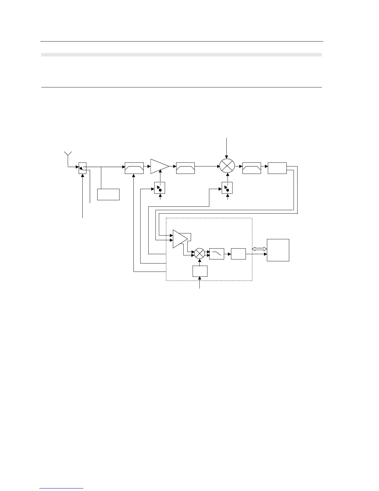
Receiver Path, Detailed Circuit Description
See Figure 4.1-6.
Figure 4.1-6 Receive Path Circuit Diagram
Antenna Switch
The signal from the antenna is routed to the receiver input via the transmitter harmonic fil-
ter (C5016, L5008, C5015 and C5011 ), an equivalent quarter wave line (L5007 with
C5011 and C5020) and the low pass (C5020, L5011, C5022 and C5021) for spurious
response improvement. Isolation to transmitter frequencies at this point is better than
35dB; attenuation of the wanted Rx signal is typically 0.7dB.
Limiter
Diode D2100 limits the level of incoming high power signals (> 5dBm) to prevent damage
to the receiver front end.
Redcap2
DSP
GP06
GP05
From Main Synthesizer
LO level = 0 dBm
489.65 – 539.65 MHz
Balun
XTAL
IF Filter
109.65MHz
IL=2dB
Post-selection Filter
IL=2dB
Pre-selection Filter
IL=2dB
Integrated
LNA
Gain=18dB
I=7.5 mA
Mixe
Gain= -6dB
I=5.0m
LO Level=-4dBm
AntSW
IL=0.7dB
From
TETRA
TX
From
VCNTO
pin of
WPIC
FE_CNTL
Baseband
Filter
A/D
Divide
by 2
WPIC
SSI
I=13mA
From 2
nd
LO
2.775V
2.775V
XTALWARP
Q2200 Q2400
Limiter

 Loading...


