Topaz T2688/T200, T2988/T205 L3 Circuit Description
8
Motorola Proprietary Information
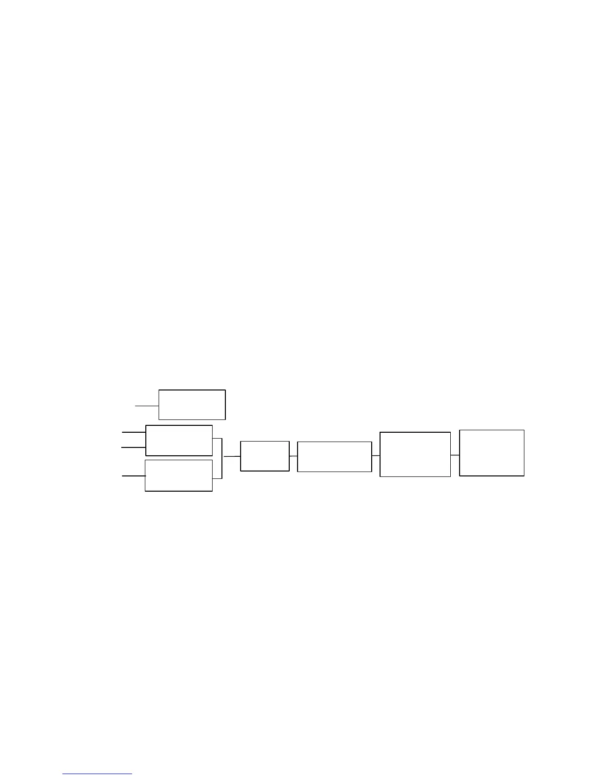
TRANSMIT
30. There are 2 sources of input audio:
31. Auxiliary Microphone is fed in through J40 External Connector Pin1 and is fed
through Jumper Connector J8 (JTAG Use), and is amplified through the BQ5 circuit,
supported by the voltage DVCC. The input signal is fed onto the base of Audio
AmpBQ5, amplified, and fed out of the collector as AUXI.
32. The Internal Microphone X1, uses the circuit R14 / R15 / C22 / C23 / R17 / R18 to
provide microphone biasing, the biasing support voltage being fed from the VEGA IC
from Pin 26. (Gain approximately 27dBm)Voltage suppressers U48 and U49 provide
ESD protection to the circuit.
33. If both inputs are active then, output signal from the internal microphone will be used.
34. The input analogue audio is then routed to the VEGA IC Pins 28 & 29. Within the
VEGA the analogue signal will be driven through a PGA with a gain of between –
12dB to +12dB in 1dB steps.
35. A Sigma-Delta Modulator converts the signal from analogue to Digital, sampled at
1Mhz. The signal is the decimated and the sampling rate taken down to signal
samples at 8Khz.
36. Once again, as in RECEIVE, the loop between the VEGA IC and the GEMINI IC is
put in place for standard data processing.
37. The transmitted signal is sent to the Gemini IC over the Voice-band VDR Line
VEGA Pin 14 and is clocked by VCLKRX Pin 16. The signals are then received by
the Gemini IC on Pins 97 & 98 respectively. Synchronisation is achieved using the
frame synch signal VFSRX (VEGA Pin 13 / GEMINI Pin 96.
38. After processing, the Base-band signal information is transferred back to the VEGA
IC using the base-band lines, BFSR / BDR / BCLKR / (VEGA Pins 6, 4 & 5 and
GEMINI Pins 74 / 75 / 76 respectively)
39. Within the VEGA IC, the received information will now be modulated by GMSK.
 Loading...