2-16
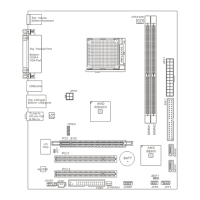
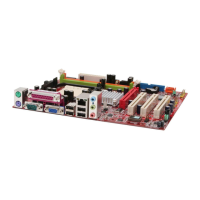
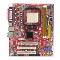
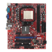
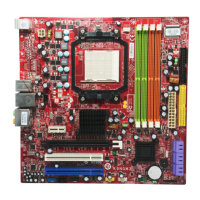
MS-7501 Mainboard
PIN SIGNAL DESCRIPTION
1 HD_LED + Hard disk LED pull-up
2 FP PWR/SLP MSG LED pull-up
3 HD_LED - Hard disk active LED
4 FP PWR/SLP MSG LED pull-up
5 RST_SW - Reset Switch low reference pull-down to GND
6 PWR_SW + Power Switch high reference pull-up
7 RST_SW + Reset Switch high reference pull-up
8 PWR_SW - Power Switch low reference pull-down to GND
9 RSVD_DNU Reserved. Do not use.
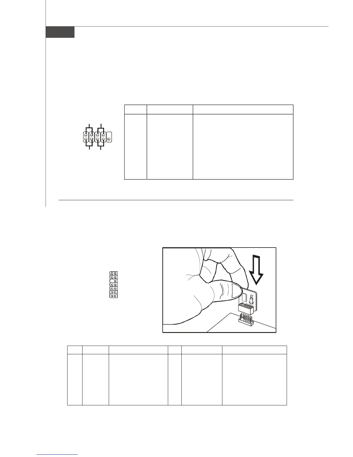
JFP1 Pin Definition
Front Panel Connector: JFP1
This connector is provided for electrical connection to the front panel switches/LEDs
and is compliant with Intel
®
Front Panel I/O Connectivity Design Guide.
Pin Signal Description Pin Signal Description
1 LCLK LPC clock 2 3V dual/3V_STB 3V dual or 3V standby power
3 LRST# LPC reset 4 VCC3 3.3V power
5 LAD0 LPC address & data pin0 6 SIRQ Serial IRQ
7 LAD1 LPC address & data pin1 8 VCC5 5V power
9 LAD2 LPC address & data pin2 10 KEY No pin
11 LAD3 LPC address & data pin3 12 GND Ground
13 LFRAME# LPC Frame 14 GND Ground
TPM Connector: JTPM1 (Optional)
This connector is designed to connect an optional TPM (Trusted Platform Module).
Please refer to the TPM security platform manual for more details.
1
2
9
10
JFP1
HDD
LED
Reset
Switch
Power
LED
Power
Switch
+
+
+
- -
-
2 1
14 13
JTPM1