µP D65026
20
1
21
40
60
41
61
80
IC2
PSG/10448/1
BEC
RPR 550IS Series
TM1188 Issue 1Page 5 - 22
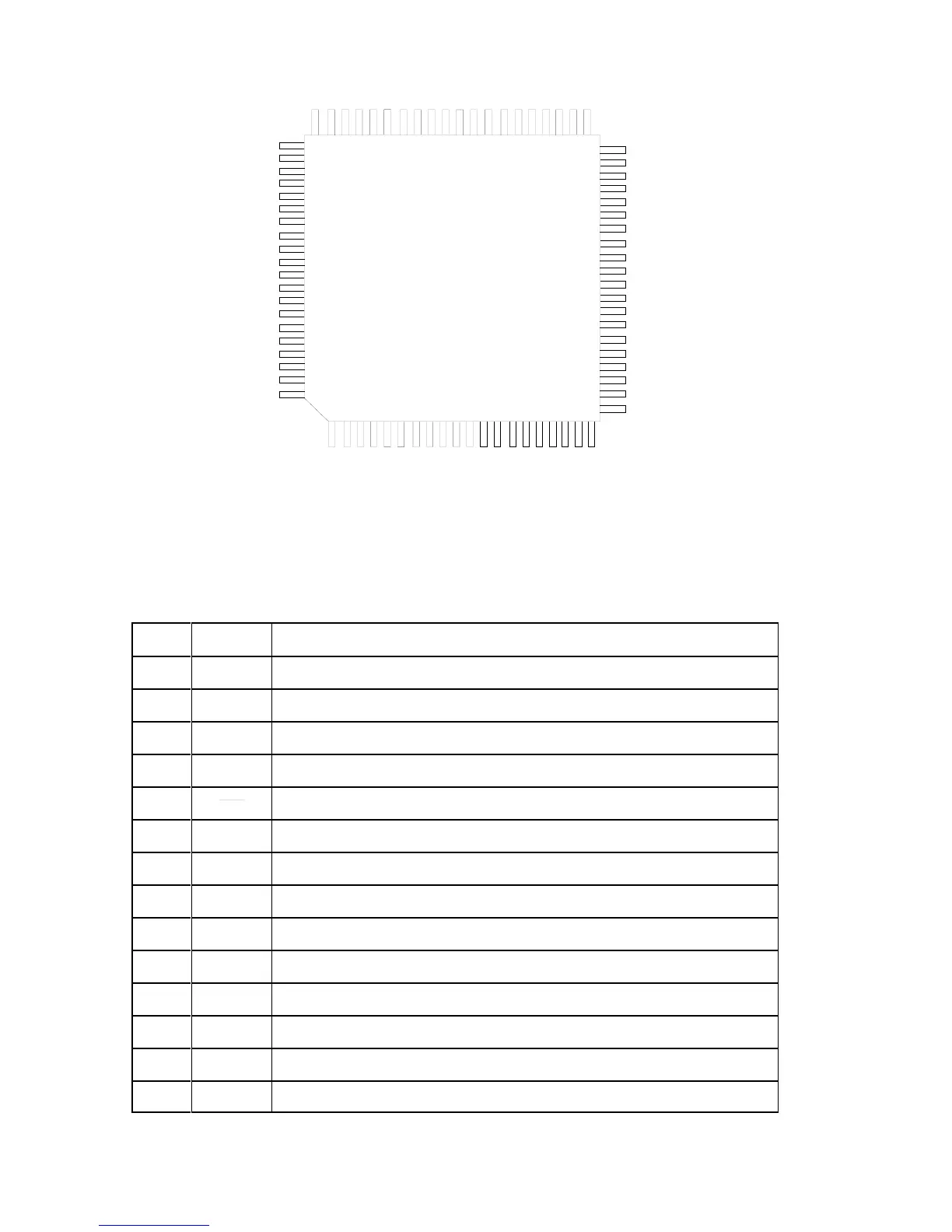
Figure 7: IC2, Gate Array Pin Configuration
Table 7: IC2, Gate Array Pin Connections
PIN NAME DESCRIPTION
1 OSEN Oscillator cell enable
3 CLK Clock input: 512 baud = 32.768kHz, 1200 baud = 38.400kHz
5 RESB Reset input: 0 = reset
7 DIN Data input
9 Radio enable: 0 = radio on, 1 = radio off
10 V
DD
1 Low voltage supply rail (0.9V - 1.5V)
11 V
SS
Ground
13 TON Beep drive: 0 = transducer on, 1 = transducer off
15 VIB Vibrate motor drive: 0 = motor on, 1 = motor off
17 OFF V
DD
enable: 0 = V
DD
on, 1 = V
DD
off
19 RSO Reset out: 0 = µP enabled, 1 = µP reset
21 LP2 LED enable
22 V
SS
Ground
25 CS Chip select: 0 = chip selected, 1 = chip deselected