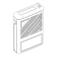
RPR 550IS Series
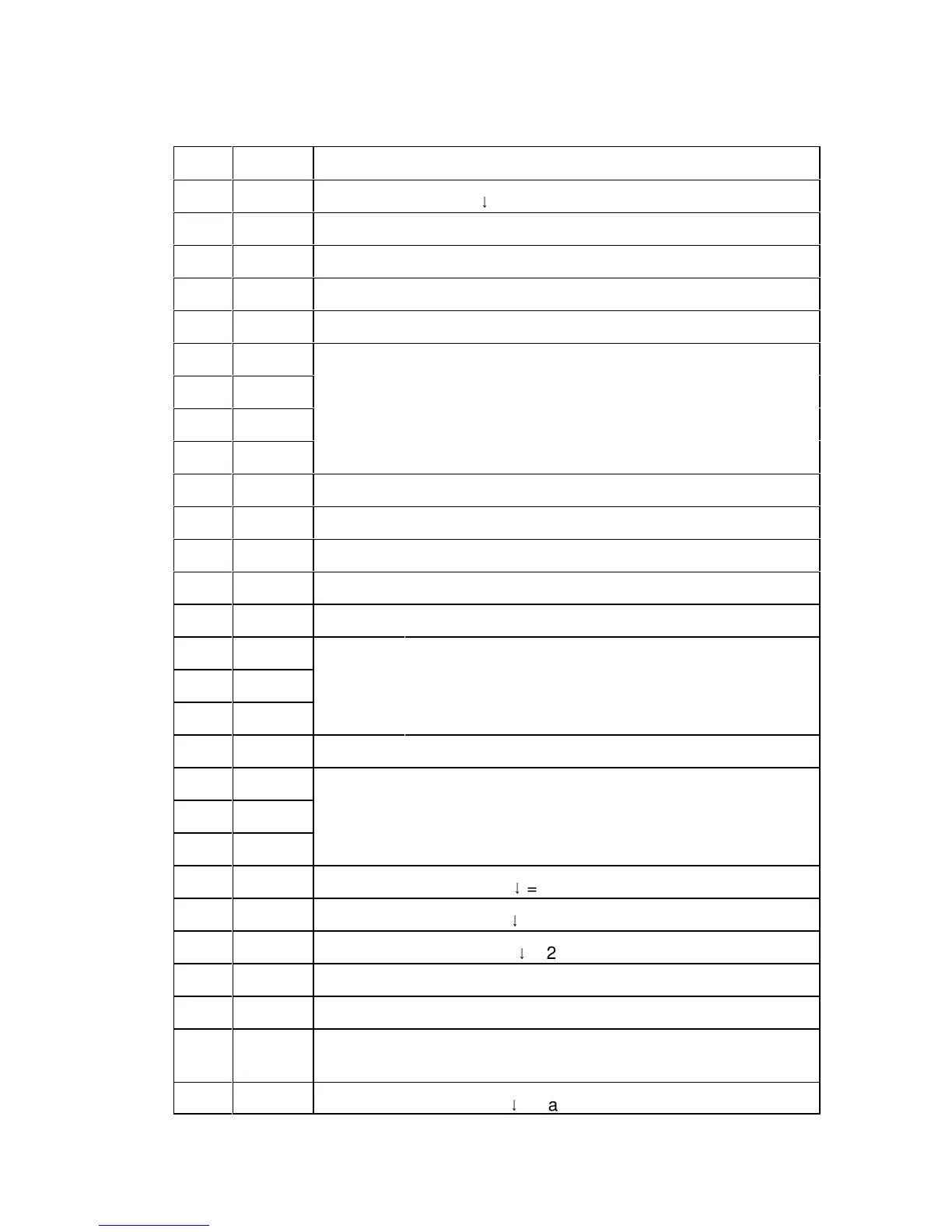
Table 7: IC2, Gate Array Pin Connections
PIN NAME DESCRIPTION
TM1188 Issue 1 Page 5 - 23
26 E Data transfer clock:
= data transfer
27 RW Read/Write: 0 = write to chip, 1 = read from chip
28 RS Register select: 0 = data register, 1 = address/status
30 V
SS
Ground
31 V
DD
2 µP supply rail
35 DA0
Tri-state bi-directional buffer: bi-directional data bus
DA3 = most significant bit
DA0 = least significant bit
36 DA1
37 DA2
38 DA3
39 V
SS
Ground
42 TSF 128Hz output
50 V
SS
Ground
51 V
DD
1 Low voltage supply rail (0.9V - 1.5V)
53 ON On enable: 0 = switch on, 1 = quiescent mode
55 S1I `On'
Switch inputs: 0 = switch closed, 1 = switch open57 S2I `Off'
59 S3I `Mute'
62 V
SS
Ground
63 S10
Tri-state, switch outputs: 0 = switch closed, Z = switch open
(Z = high impedance output)
64 S20
65 S30
66 DTI Tri-state, data interrupt:
= data interrupt
67 SWI Tri-state, switch output:
= switch operation
68 TMI Tri-state, timer interrupt:
= 2s elapsed
70 V
SS
Ground
71 V
DD
2 µP supply rail
72 SYN Tri-state, sync word detected: 0 = sync word present in data
register
76 SCK Tri-state, sample clock:
= sample point of data bit