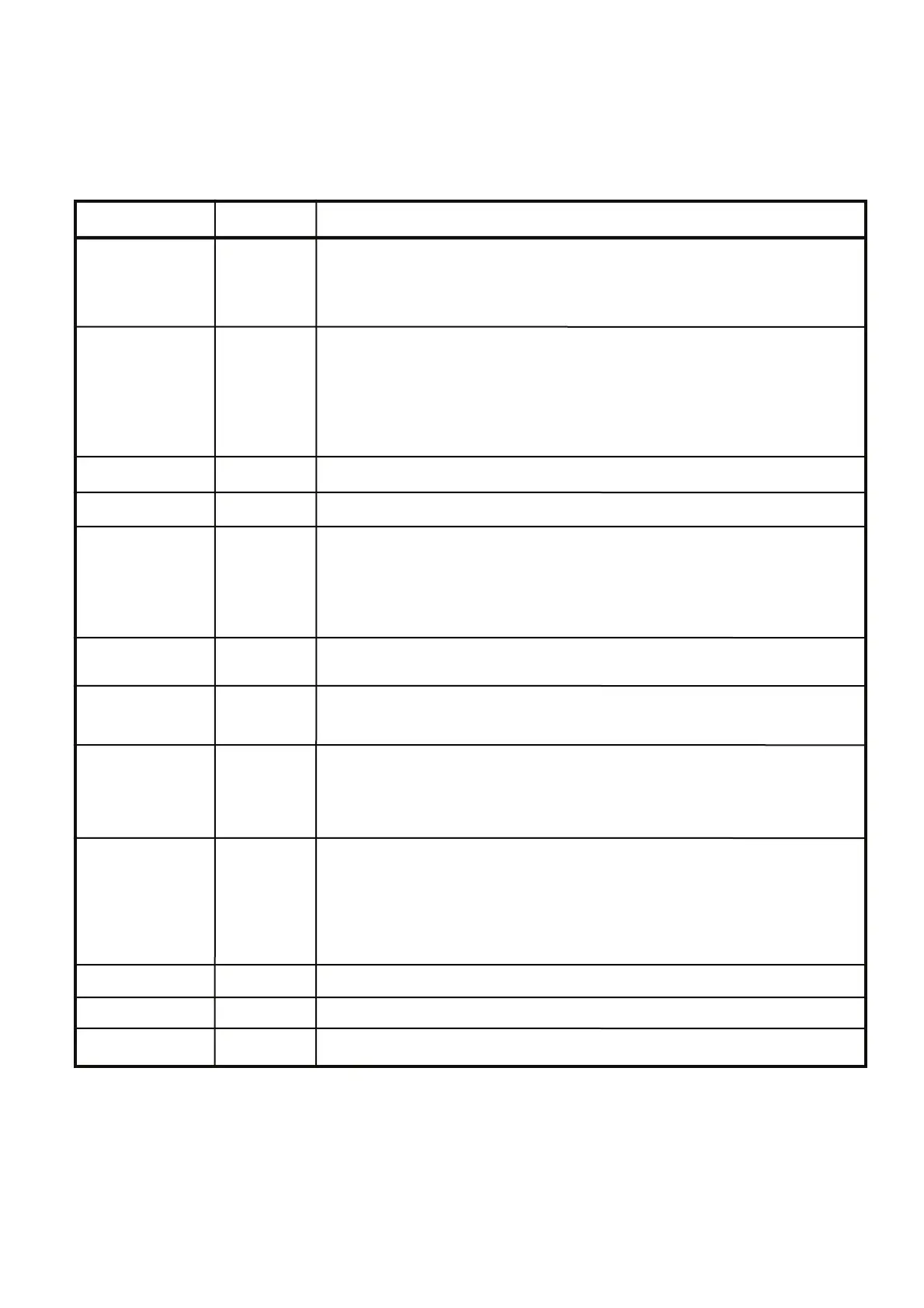
CLK, /CLK Input
Clock: CLK and /CLK are differential clock inputs. All address and control
input signals are sampled on the crossing of the positive edge of CLK and
negative edge of /CLK. Output (read) data is referenced to the crossings of
CLK and /CLK (both directions of crossing).
CKE
Input
Clock Enable: CKE controls Power Down and Self Refresh.
Taking CKE LOW provides Precharge Power Down or Self Refresh (all banks idle),
or Active Power Down (row active in any bank).
Taking CKE HIGH provides Power Down exit or Self Refresh exit.
After Self Refresh is started, CKE becomes asynchronous input.
Power Down and Self Refresh is maintained as long as CKE is LOW.
/CS Input Chip Select: When /CS is HIGH, any command means No Operation.
/RAS, /CAS, /WE Input Combination of /RAS, /CAS, /WE defines basic commands.
A0-12 Input
A0-12 specify the Row / Column Address in conjunction with BA0,1. The
Row Address is specified by A0-12. The Column Address is specified by
A0-9(x8) and A0-8(x16). A10 is also used to indicate precharge
option. When A10 is HIGH at a Read / Write command, an Auto Precharge
is performed. When A10 is HIGH at a Precharge command, all banks are precharged.
BA0,1 Input
DQ0-7 (x8),
DQ0-15 (x16),
Input / Output
DQS (x8)
Vdd, Vss Power Supply Power Supply for the memory array and peripheral circuitry.
VddQ, VssQ Power Supply VddQ and VssQ are supplied to DQ, DQS buffers.
Bank Address: BA0,1 specifies one of four banks to which a command is applied.
BA0,1 must be set with Active, Precharge, Read, Write commands.
Data Input/Output: Data bus
Data Strobe: Output with read data, input with write data. Edge-aligned
with read data, centered in write data. Used to capture write data.
For the x16, LDQS corresponds to the data on DQ0-DQ7; UDQS
correspond to the data on DQ8-DQ15
SYMBOL TYPE DESCRIPTION
DM (x8)
Input
Input Data Mask: DM is an input mask signal for write data. Input data
is masked when DM is sampled HIGH along with that input data
during a write access. DM is sampled on both edges of DQS.
Although DM pins are input only, the DM loading matches the DQ
and DQS loading. For the x16, LDM corresponds to the data on DQ0-DQ7;
UDM corresponds to the data on DQ8-DQ15.
Input / Output
VREF Input SSTL_2 reference voltage.
UDQS, LDQS (x16)
UDM, LDM (x16)
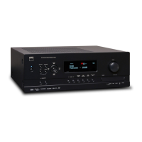
IC 912 : A3S56D40FTPG5 (HDMI / DDR SDRAM)
PIN FUNCTION
2-18
 Loading...