© National Instruments | B-29
M Series User Manual
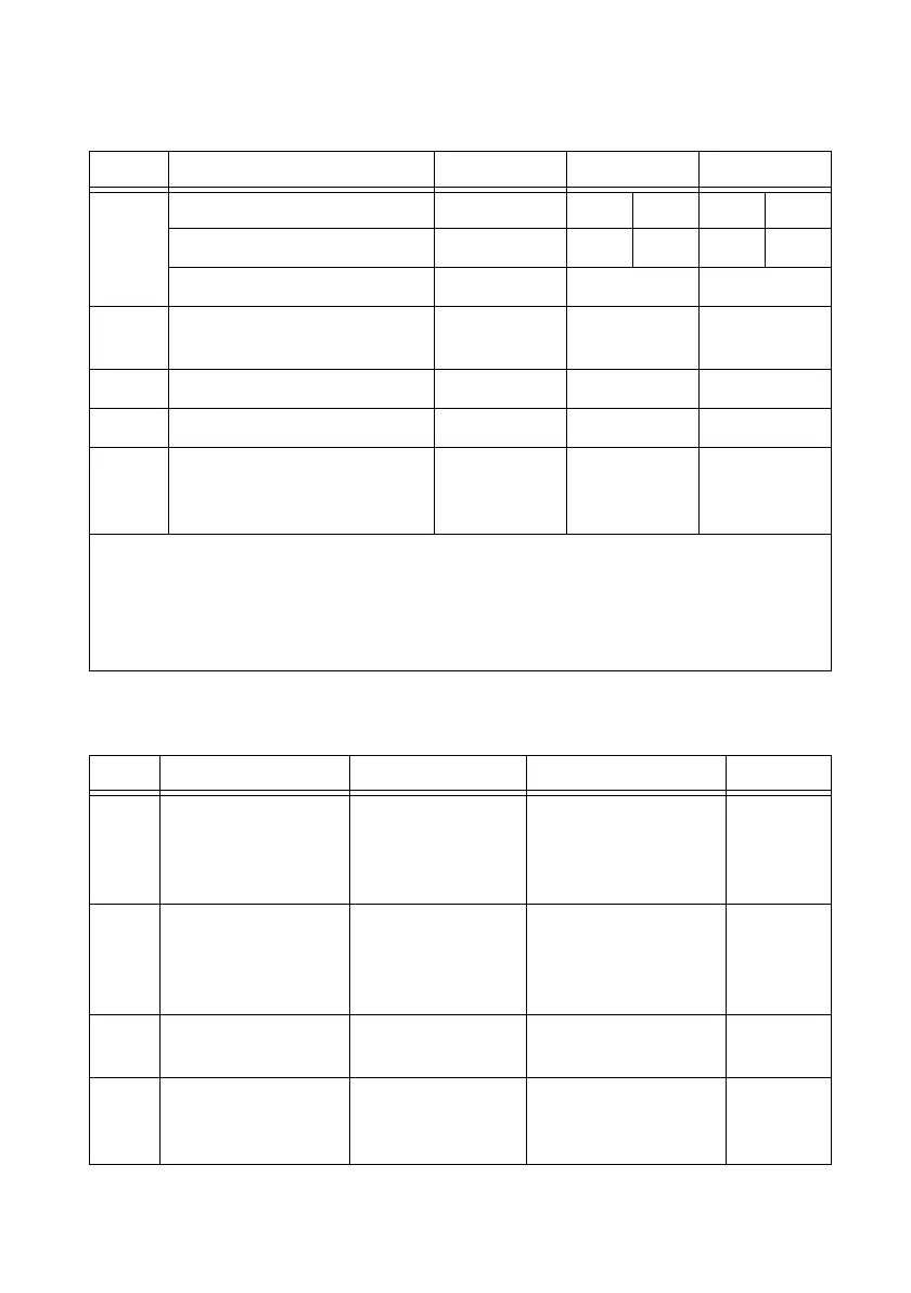
Table B-22. DI Timing Delays
Time From To Min (ns) Max (ns)
t
3
*
PFI PFI_i 5.2 6.2 18.2 22.0
RTSI RTSI_i 2.0 2.5 5.0 6.0
PXI_STAR PXI_STAR_i 1.5 3.5
t
4
PFI_i, RTSI_i, PXI_STAR_i,
or other internal signal
DI Sample
Clock
3.5 9
t
7
P0 P0_i 4.7 20.1
t
8
DI Sample Clock PFI (output) 8.0 29.8
t
9
†
PFI (output) high PFI (output)
low
One period of
80 MHz
Timebase
Two periods
of 80 MHz
Timebase
*
The delay ranges given for PFI and RTSI represent the fastest and slowest terminal routing within the
trigger group for a given condition (maximum or minimum timing). This difference can be useful when
two external signals will be used together and the relative timing between the signals is important.
†
When DI Sample Clock is routed to a PFI output pin, the pulse width of the output is independent of
the pulse width of the input. The pulse width is specified in a number of periods of the 80 MHz Timebase
Table B-23. DI Timing Requirements
Time Requirement Condition Min (ns) Max (ns)
t
1
PFI, RTSI, or
PXI_STAR
minimum period
When used as DI
Sample Clock
NI 622x devices:
1000.0
NI 625x/628x
devices: 100.0
—
t
2
PFI, RTSI, or
PXI_STAR
minimum pulse
width
When used as DI
Sample Clock
12.0 —
t
5
Setup time from P0_i
to DI Sample Clock
— 1.5 —
t
6
Hold time from DI
Sample Clock to
P0_i
— 0 —
 Loading...