EasyManuals Logo

National Instruments ZYNQ XC7Z020-1CLG484C User Manual

National Instruments ZYNQ XC7Z020-1CLG484C
63 pages
To Next Page IconTo Next Page
To Previous Page IconTo Previous Page
Page #50 background imageLoading...
Page #50 background image
50 | ni.com | NI Digital System Development Board User Manual
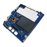
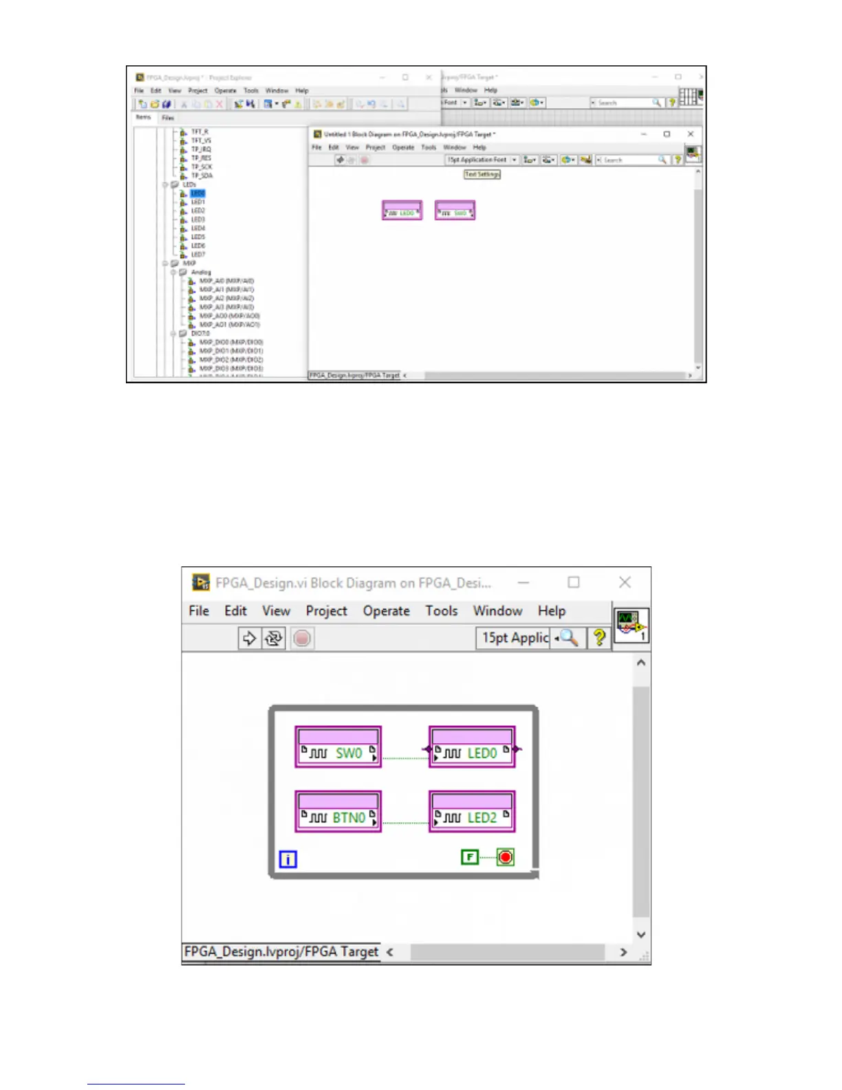
5. In the LabVIEW block diagram, wire SW0 output to the LED0 input.
6. In the Project Explorer window FPGA Target (DSDB, Digital Systems Development
Board) tree view, select BTN0 and LED2 and drag them onto the block diagram.
7. In the LabVIEW block diagram, wire BTN0 output to the LED2 input.
8. Add a While Loop around the resources.
9. Wire a false constant to the stop condition of the While Loop as shown below.
10. Save the VI as
FPGA_Design.vi.

Questions and Answers:

Question and Answer IconNeed help?

Do you have a question about the National Instruments ZYNQ XC7Z020-1CLG484C and is the answer not in the manual?

National Instruments ZYNQ XC7Z020-1CLG484C Specifications

General IconGeneral
BrandNational Instruments
ModelZYNQ XC7Z020-1CLG484C
CategoryMotherboard
LanguageEnglish