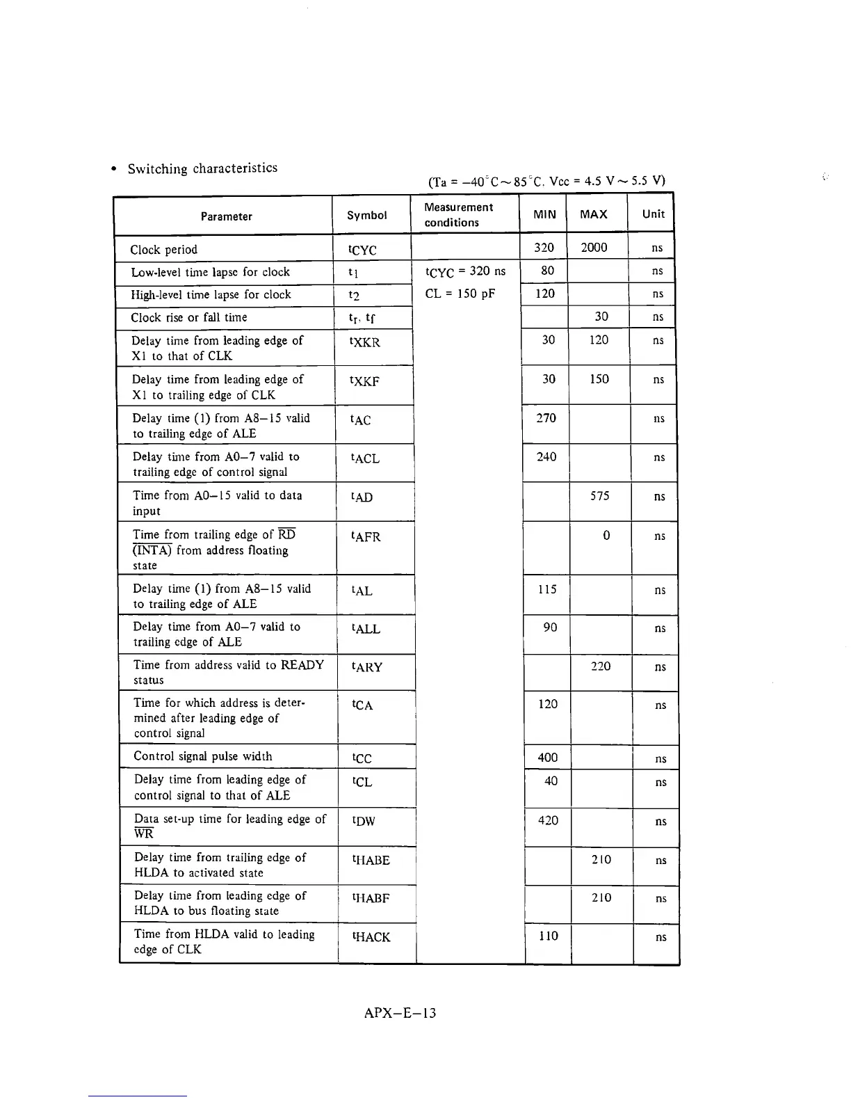
Switchirlg characteristics
(Ta
=
-40'C- 85 "C. Vcc
=
4.5
V
--
5.5
V)
Parameter
Measurement
I
Symbol
I
conditions
I
MIN
(
MAX
I
Unit
I
XI to trailing edge of CLK
Delay time
(1)
from A8-15 valid
to trailing edge of ALE
Delay time from AO-7 valid to
trailing
edgc of control signal
Clock period
Low-level
time lapse for clock
High-level time lapse for clock
Time
from AO-15 valid to data
I
1
tCYC
t
1
t2
Time from address valid to READY
t~lty
status
I
input
Time from
trailing edge of
(MA) from address floating
state
Delay time
(1)
from A8-15 valid
to trailing edge of ALE
Delay time from AO-7 valid
ro
trailing cdge of
ALE
Time
for which address is deter-
mined after leading edge of
control
signal
tcyc
=
320 ns
CL
=
150
pF
Clock rise or fall time
I
trtf
t
AFR
tXL
t
ALL
Control signal pulse width
I
tCC
I
30
30
Delay time from leading edge of
XI to that of CLK
Delay time from leading edge of
Delay time from leading edge of
control signal to that of
ALE
I
ICL
I
320
80
120
tXKR
tXKF
Data set-up time for leading edge of
I
t~w
I
30
120
150
ns
ns
ns
2000
APX-E-
13
ns
ns
ns
Delay time from trailing edge of
HLDA to activated state
Delay time from leading edge of
HLDA to bus floating state
tHABE
tI-IABF
Time from HLDA valid
to
leading
1
IHACK
cdge of CLK