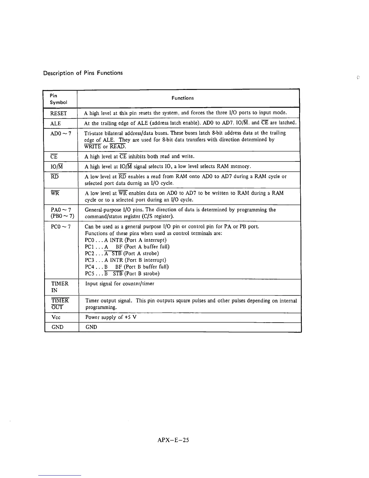
Description of Pins Functions
Pin
Symbol
RESET
ALE
ADO
-
7
CE
IO~
-
RD
RiF
PA0
--
7
(PBO
--
7)
PC0
-
7
TIMER
IN
TDlER
-
OUT
Vcc
GND
Functions
A high level at this pin resets the system, and forces the three
110
ports to input mode.
At the trailing edge of
ALE
(address larch enable). ADO to AD7. IO/M. and
CE
are latched.
Tri-state bilateral
addressldata buses. These buses latch 8-bit address data at
the
trailing
edge of
ALE.
They are used for &bit data transfers with direction determined by
--
WRITE
or READ.
A high level at
CE
inhibits both read and write.
A
high level at
IO~
signal selects
10,
a low level selects
RAh1
memory.
A low level at
enables a read from
RAM
onto ADO to AD7 during a
RAM
cycle or
selected port data durnig an
110 cycle.
A
low level at menables data on ADO to AD7 to be wrilten to
RAM
during a RAM
cycle or to
a
selected port during
an
110 cycle.
General-purpose
110 pins. The direction of data is determined by programming the
command/status register (CIS register).
Can be used as a general purpose
110 pin or control pin for PA or P13 port.
Functions of these pins when used as control terminals are:
PC0
.
.
.
A NTR (Port A interrupt)
PC1
. .
.
A
BF
(Port
A buffer full)
PC2
.
. .
A STB (Port
A
strobe)
PC3
. .
.
A
INTR (Pon B interrupt)
PC4
. . .
B
BF (Port
B
buffer full)
PC5
. . .
B
STB (Port
B
strobe)
Input signal for
counterltimer
Timer output signal. This pin outputs square pulses and other pulses depending on internal
programming.
Power supply of
+5
V
GND