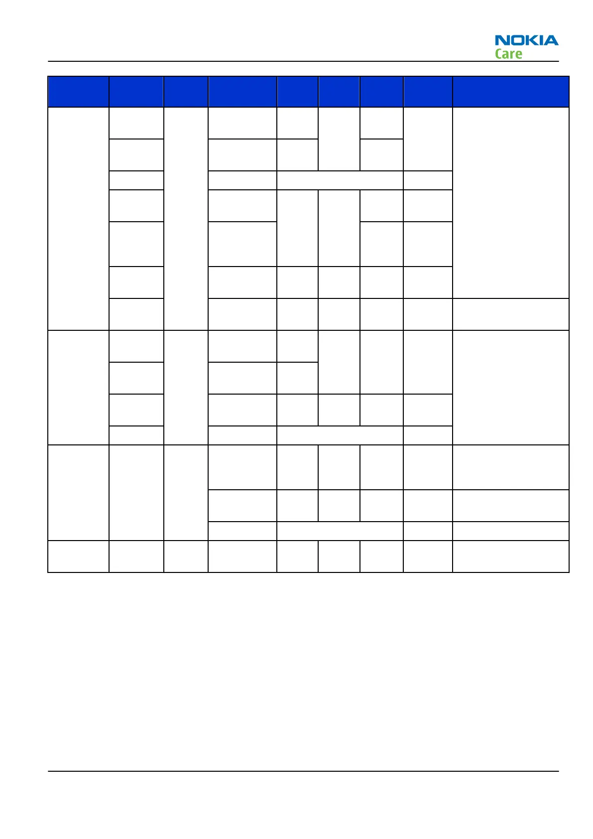
Signal
name
From To Parameter Min Typ Max Unit Function
AFC UEMCLit
e
VCTCX
O
Voltage Min 0.0 0.1 V Automatic Frequency
Control signal for
VCTCXO
Programmable
(AFCOUT
)
Max 2.4 2.55
Resolution 11 bits
Load
resistance
1 kW
and
capacitanc
e
100 nF
Source
Impedance
200 W
Output
impedance
10 MW Path powered down
TxC UEMCLit
e
RF-IC Voltage Min 0.1 V Transmitter power
level and ramping
control, Ref UEMCLite
RF converter
specification
(AUXOUT
)
Max 2.4
Source
Impedance
200 W
Resolution 10 bits
VCXOTEMP RF-IC UEMCL
ite
Input
voltage
range
0 2.7 V
Input
resistance
900 6000 Ohm
Resolution 10 bits
PATEMP RF-IC UEMCL
ite
Voltage at
-20oC
1.57 V Usage depends of the
RF design
LCD interface
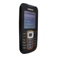
The display is controlled by phone processor UPP.
The main LCD module is connected to the PWB by a 24-pin board-to-board connector.
The sub LCD module is connected to the PWB by a 10-pin board-to-board connector.
Keyboard
A 5 X 5 matrix keyboad consists of 21 keys, one 10-channel integrated passive filiter arrays with downstream
ESD protection of >8KV connect the matrix keyboard to UPP.
RM-340; RM-341
System Module
Issue 1 COMPANY CONFIDENTIAL Page 6 –15
Copyright © 2007 Nokia. All rights reserved.