NOVATECH INSTRUMENTS 12 409C Manual Rev 1.12
maximum of 1020/Fs where Fs is the Synthesis Clock
frequency as displayed with the ‘q’ command.
NOTE:
Entering a step time t that is larger than the maximum
allowed value for t will result in the step time being set
to the maximum allowed value.
4.22 Total Sweep Time. To compute the total time a
sweep will take, first compute the total number of steps.
This is the begin frequency minus the end frequency di-
vided by the frequency step size. The sweep time will
then be the number of steps times the step time.
4.23 Running a Sweep. To execute a sweep the user
must first enable sweeps using the ‘SWENBN x’ com-
mand where x can be E for enabled and D for disabled.
Once enabled the sweep must be triggered with a rising
edge on the trigger input to start a rising sweep and a
falling edge to start a falling sweep . Triggering is done
using the ‘PPn 0’ and “PPn 1’commands or sending the
‘PPn x’ command and then applying a 3.3V signal on
connector J8. See example on page 6.
4.24 Sweep Default Settings. The default sweep set-
tings for output channel 0 are as follows:
F0=10.0000000 P0=0.00 V0=1.000
(Begin frequency = 10MHz, Phase = 0, Vout = 1Vpp)
SWEF0=150.0000000
(Ending frequency = 150MHz)
SWRSF0=1.0000000 SWFSF0=1.0000000
(Rising and falling frequency steps = 1 MHz)
SWRST0=1.000 SWFST0=1.000
(Rising and falling time steps = 1 microsecond)
SWMD0=S SWENB0=D
(Sweep mode set to Ramp up and Step down. Sweep Enable/
Disable set to Disable)
4.25 Sending Sweep Commands. It is recommended
that the SOF8_409 software command menu be used to
set the sweep parameters and run the sweep. Sending a
‘q’ command will display the current settings of the
sweep parameters on all output channels.
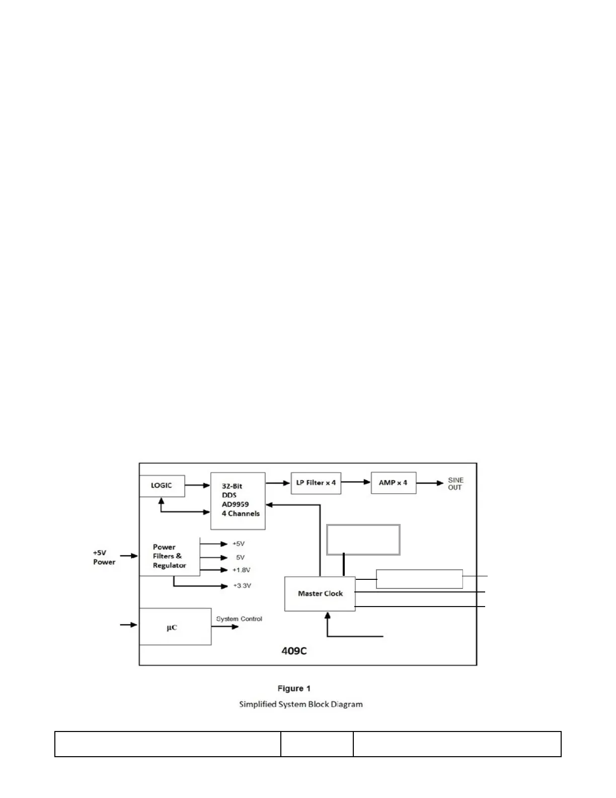
5.0 THEORY OF OPERATION
5.1 Block Diagram. Please refer to the simplified Sys-
tem Block Diagram below for the following discussion.
5.2 DDS. At every cycle of the 409C system clock, the
AD9959 integrated circuit increments the phase of an
internal register by a value calculated from the frequency
command and sent to the AD9959 by the microcontrol-
ler. The AD9959 converts this phase value to a sinusoi-
dal amplitude level and then sets the values of on-chip
Rear BNC & /R
Rear BNC
Rear SMA
Clock
Select
Command
Internal TCXO
Serial Commands
/R Daughter board
Note: Master Clock is the synthesizer clock prior
to applying the AD9959 clock mulplier
 Loading...