NXP Semiconductors
S32K344
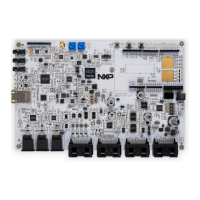
White Board
J32-1 D_IN_3 PEPS wake up J32-11 HB_OUT2 HB2001 out
Table 2. Signals definitions of J32...continued
The signals definitions of J33 are listed in the following table:
PIN Label Function PIN Label Function
J33-10 GND GND J33-20 VBAT1 12V power
J33-9 GND GND J33-19 VBAT1 12V power
J33-8 NC NC J33-18 LS_DRV_OUT_
8
Low side output
J33-7 NC NC J33-17 LS_DRV_OUT_
7
Low side output
J33-6 VBAT3 12V power J33-16 LS_DRV_OUT_
6
Low side output
J33-5 VBAT3 12V power J33-15 LS_DRV_OUT_
5
Low side output
J33-4 HS_DRV_OUT4 High side output J33-14 LS_DRV_OUT_
4
Low side output
J33-3 HS_DRV_OUT3 High side output J33-13 LS_DRV_OUT_
3
Low side output
J33-2 HS_DRV_OUT2 High side output J33-12 LS_DRV_OUT_
2
Low side output
J33-1 HS_DRV_OUT1 High side output J33-11 LS_DRV_OUT_
1
Low side output
Table 3. Signals definitions of J33
The signals definitions of J36 are listed in the following table:
PIN Label Function PIN Label Function
J36-10 GND GND J36-20 +5V_OUT2 +5V power
J36-9 ISELED_P ISELED
Interface
J36-19 ISELED_N
ISELED
Interface
J36-8 MSDI_SP5 Switch input J36-18 MSDI_SG5 Switch input
J36-7 MSDI_SP4 Switch input J36-17 MSDI_SG4 Switch input
J36-6 MSDI_SP3 Switch input J36-16 MSDI_SG3 Switch input
J36-5 MSDI_SP2 Switch input J36-15 MSDI_SG2 Switch input
J36-4 MSDI_SP1 Switch input J36-14 MSDI_SG1 Switch input
J36-3 MSDI_SP0 Switch input J36-13 MSDI_SG0 Switch input
J36-2 A_IN_2 ADC input J36-12 D_IN_2 Digital input
J36-1 A_IN_1 ADC input J36-11 D_IN_1 Digital input
Table 4. Signals definitions of J36
The signals definitions of J31 are listed in the following table:
UM11919 All information provided in this document is subject to legal disclaimers. © 2023 NXP B.V. All rights reserved.
User manual Rev. 1.0 — 11 April 2023
COMPANY PUBLIC 5 / 32
 Loading...