ON Semiconductor
www.onsemi.com
13
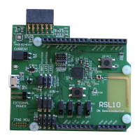
For the QFN board, use the jumpers on pin headers P4, P7 and P10 to select a power supply option as show in
Table 2.
3.4 LEVEL TRANSLATORS
The board has level translators for the DIO signals of RSL10, including the clock signal. The level translators
facilitate interfacing to external devices that operate at a higher voltage than RSL10.
VDDO and 3.3 V are two different power rails. The translator allows a logic signal on the VDDO side to be
translated to either a higher or a lower logic signal voltage on the 3.3 V side, and vice-versa.
The level translation circuitry consists of components
U4 and the 2x4 header. Signals are translated from the VDDO
voltage reference to 3.3 V (default) voltage provided by the regulator output or by an external supply. The VDDO
voltage is configured by the pin on header
P11 (located on the board edge) to either VBAT_DUT, 3.3 V or other level
within the VDDO voltage range, which is 1.1 to 3.3 V.
The NLSX5014 level translators are bi-directional. They have the following features:
• Wide voltage operating range: 0.9 V to 4.5 V
• VDDO and 3.3 V are independent
• VDDO can be equal to, or less than, 3.3 V when connected to the power rail
To enable the level translators, populate the 0W resistor on positions R31 and R33. By default, the level translators
are disabled.
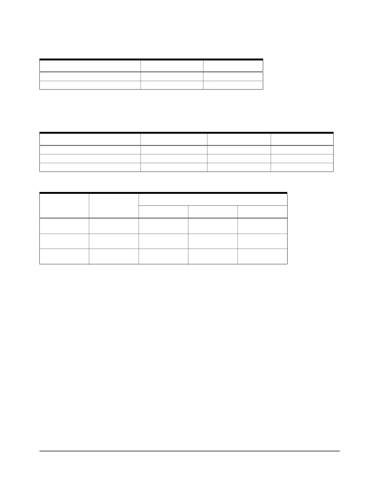
External Power supply with regulator 1&2 3&4
External Power supply without regulator 2&3 5&6
Table 2. Power Supply Selection for QFN
Power Source Jumper Position on P4 Jumper Position on P7 Jumper Position on P10
Micro USB port with regulator 1&2 2&3 1&2
External Power Supply with regulator 3&4 2&3 1&2
External Power Supply without regulator 1&2, 5&6 2&3 2&3
Table 3. Minimum/Maximum External Regulated Voltages
Power Supply Header
Input Voltage
Minimum Typical Maximum
RSL10 and J-Link
OB MCU
EXT-PSU
Regulated
3.3 V 3.6 V 12.0 V
RSL10 and J-Link
OB MCU
USB
5.0 V
RSL10
EXT-PSU
Unregulated
1.1 V 1.25 V 3.6 V
Table 1. Power Supply Selection for WLCSP (Continued)
Power Source Jumper Position on P6 Jumper Position on P8