www.onsemi.com
6
CHAPTER 2
2.Overview
2.1 INTRODUCTION
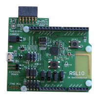
The RSL10 Evaluation and Development Board is used for evaluating the RSL10 SoC and for application
development. The board provides access to all input and output connections via 0.1" standard headers. The on-board
communication interface circuit provides communication to the board from a host PC. The communication interface
translates RSL10 SWJ-DP debug port signals to the USB of the host PC. There is also an on-board 4-bit level shifter
for debugging; it translates the I/O signal level of RSL10 to the 3.3 V digital logic level. It is not enabled by default;
you enable it when it is needed.
2.2 EVALUATION AND DEVELOPMENT BOARD FEATURES
The Evaluation and Development Board enables developers to evaluate the performance and capabilities of the
RSL10 radio SoC in addition to developing, demonstrating and debugging applications.
Key features of the board include:
• J-Link onboard solution provides a SWJ-DP (serial-wire and/or JTAG) interface that enables you to debug
the board via a USB connection with the PC
• Alternate onboard SWJ-DP (serial-wire and/or JTAG) interface for ARM® Cortex®-M3 processor
debugging
• Access to all RSL10 peripherals via standard 0.1" headers
• Onboard 4-bit level translator to translate the LPDSP32 debug interface at low voltage to a 3.3 V JTAG
debugger
• Antenna matching and filtering network
• Integrated PCB antenna
In addition, the QFN board provides:
• Compliance with the Arduino form factor
• Support for PMOD (i.e., J4 is a standard connector)