www.onsemi.com
17
APPENDIX A
A.WLCSP Connectors
A.1 OVERVIEW
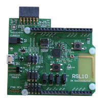
This appendix lists all connectors on the Evaluation and Development Board. The sections that follow provide
descriptions for:
• Jumpers and their possible configurations
• Headers
• Switches and their possible configurations
• Connectors
A.2 CONFIGURATION HEADER JUMPERS
A.3 HEADERS
A.4 SWITCHES
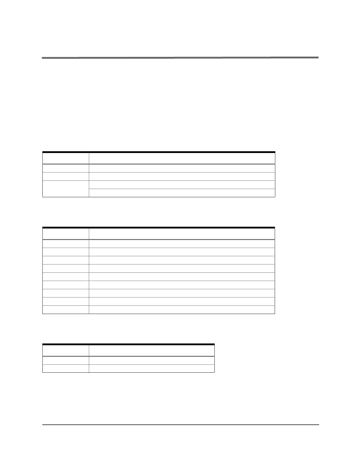
Table 4. Jumper Descriptions
Designator Description
P6 Regulated or Unregulated power supply selection (see Table 1 on page 12)
P8 Power Source Selection (see Table 1 on page 12)
P11 VDDO selection between VBAT_DUT and V3.3
VDD_AT selection between 3.3 V and VEXT, removing R39
Table 5. Header Descriptions
Designator Description
P1 DIO signals
P2 External slow clock input header
P3 JTAG debug connection header
P4 Virtual UART port from PC
P5 Analog test header
P7 Current measurement header
P9 External power supply header
P10 Input and output of level shifter
P11 Power supply on board and supply voltage configuration header
Table 6. Switch Descriptions
Designator Description
RESET Pushbutton switch to reset RSL10
DIO5 Pushbutton switch for DIO5