www.onsemi.com
7
CHAPTER 3
3.Evaluation and Development Board
3.1 EVALUATION AND DEVELOPMENT BOARD SETUP
This section is an overview of how to configure the Evaluation and Development Board. Details of the
development board configuration are discussed later in this manual.
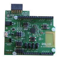
Figure 1 represents an overview of the board setup.
Figure 1. Evaluation and Development Board Setup
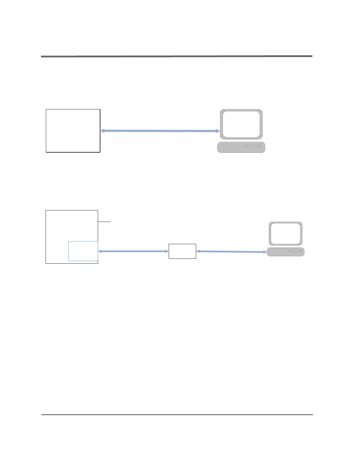
If you want to use an external J-Link debugger instead of the onboard one, connect the debugger to the JTAG
port of the WLCSP board, or to connector P2 on the QFN board, as shown in Figure 2. Notice that for this setup, you
also need a power supply.
Figure 2. Evaluation and Development Board Setup with External J-Link Debugger
3.2 E
VALUATION AND DEVELOPMENT BOARD DESIGN
The following sections detail the various sub-circuits of the RSL10 Evaluation and Development Board. The
block diagram in Figure 3 shows the locations of the various circuit sections for the WLCSP board. The block
diagrams in Figure 4 and Figure 5 show the locations of the circuit sections for the QFN board. Figure 6 and Figure 7
provide 3-dimensional illustrations of the QFN board.
RSL10
Evaluation and
Development
Board
Micro USB cable
Micro USB cable
J-Link
Debugger
10/9 Pin Connector
RSL10 Evaluation and
Development Board
P2 or JTAG
Port
Power Supply