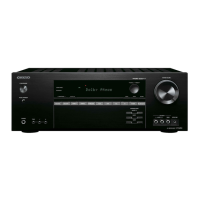
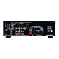
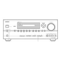
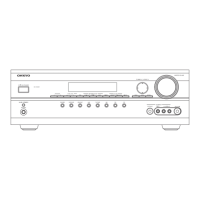
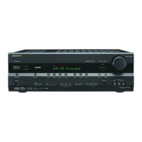
TX-SR402/8240/HT-R420
37
38
39
40
41
42
43
44
DD
DC
AUDATA2
AUDATA1
AUDATA0
LRCLK
SCLK
MCLK
Reserved.
Digital audio output 2.
Digital audio output 1.
Digital audio output 0.
Audio output sample rate clock.
Audio output bit clock.
Audio master clock.
No.
1
2
3
4
5
6
7
8
9
10
11
12
13
14
15
16
17
18
19
20
Symbol
VD1
DGMD1
AUDATA3,XMT958
WR,DS,EMWR,GPIO10
RD,R/W,EMOE,GPIO11
A1,SCDIN
A0,SCCLK
DATA7
DATA6
DATA5
DATA4
VD2
DGND2
DATA3
DATA2
DATA1
DATA0
CS
SCDIO,SCDOUT,PSEL,
GPIO9
INREQ,ABOOT
Description No. Symbol Description
Digital positive suppy
Digital suppy ground
SPDIF transmitter output. Digital audio output.
Host write strobe or host data strobe or
external memory write enable general purpose
input & output number 10.
Host parallel output enable or host parallel R/W
or external memory output enable or general
purpose input & output number 11.
Host address bit one or SPI serial control data input.
Host parallel address bit zero or serial control
port clock.
In parallel host mode these pins provide a
bi-directional databus. If a serial host mode is
selected, these pins can provide a multiplexed
address and data bus for connecting an 8-bit
external memory. Otherwise, in serial data host
mode, these pins can act as general-purpose input
or output pins that can be individually configured
and controlled by this DSP.
Digital positive supply.
Digital supply ground.
In parallel host mode these pins provide a
bi-directional data bus. If a serial host mode is
selected, these pins can provide a multiplexed
address and data bus for connecting an 8-bit
external memory. Otherwise, in serial data host
mode, these pins can act as general-purpose input
or output pins that canbe individually configured
and controlled by this DSP.
Host parallel chip select, host serial SPI chip
select.
Serial control port data input and output, parallel
port type select.
Control port interrupt request, automatic boot
enable.
21
22
23
EXTMEM,GPIO8
SDATAN1
VD3
External memory chip select or general
purpose input & output number 8.
PCM audio data input number one.
Digital positive supply.
26
27
28
29
30
31
32
33
34
35
36
24
25
LRCLKN1
CMPDAT,
SDATAN2
CMPCLK,SCLKN2
CMPREQ
LRCLKN2
CLKIN
CLKSEL
FILT2
FILT1
VA
AGND
RESET
DGND3
SCLK1,STCLK2
PCM audio input sample rate clock.
PCM audio data input number two.
PCM audio input sample rate clock.
PCM audio input bit clock.
Master clock input pin.
DSP clock select pin.
Phase locked loop filter.
Analog positive supply.
Analog supply ground.
Master reset input.
Digital supply ground.
PCM audio data input bit clock.
IC BLOCK DIAGRAM AND TERMINAL DESCRIPTIONS-5
Q701:CS493264(DSP IC)-2
TERMINAL DESCRIPTION
w
w
w
.
x
i
a
o
y
u
1
6
3
.
c
o
m
Q
Q
3
7
6
3
1
5
1
5
0
9
9
2
8
9
4
2
9
8
T
E
L
1
3
9
4
2
2
9
6
5
1
3
9
9
2
8
9
4
2
9
8
0
5
1
5
1
3
6
7
3
Q
Q
TEL 13942296513 QQ 376315150 892498299
TEL 13942296513 QQ 376315150 892498299
http://www.xiaoyu163.com
http://www.xiaoyu163.com
 Loading...