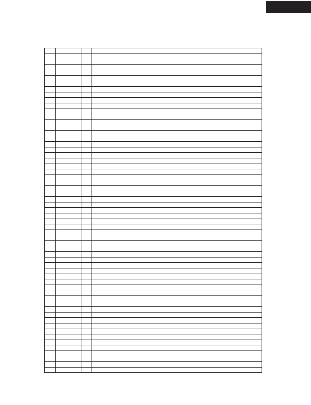
No. Terminal I/O Description
1 PROTECT I Protection circuit detection input terminal
2 VOLH I Power amplifier voltage detection terminal.
3 BAND I Region setting input terminal.
11 232TXD Not used.
15 MCRDY I Data ready detection input terminal from the sub microprocessor.
16 MCSDa I Data input terminal from the sub microprocessor.
17 MCMDA O Data output terminal to the sub microprocessor.
18 MCCLK O Serial clock output terminal to the sub microprocessor
19 ~MCRST O Reset signal output terminal to the sub microprocessor
20 HPMUT O Muting control output terminal for headphone amplifier.
21 HPIN I Input terminal to detect the connection of headphone
22 SPBRL O Speaker B relay control output terminal.
23 SEC1H O Voltage +/-B control output terminal.
24 SPACSRL O Speaker relay control output terminal for center and surround channels
25 SPAFRL O Speaker relay A control output terminal for front channels
26 POWERRL O Power source relay control output terminal
27 VCTRLA O Control signal A output terminal for the video selector switch
28 VCTRLB O Control signal B output terminal for the video selector switch
29 VMUT2 O Muting control output terminal for the video section 2
30 VMUT1 O
34 AMUT O Audio muting control output terminal
35 PLLSTB O Strobe signal output terminal to PLL IC
36 PLLSDO O Serial data output terminal to PLL IC
37 PLLCLK O Serial clock output terminal to PLL IC
38 TUMUT O Muting control output terminal for the tuner section
39 ~SD I Broadcast detection input terminal more than a muting level.
40 ~STEREO I FM stereo broadcast detection input terminal
41 SELMUT O Muting control output terminal for selector, volume and tone IC BD3811.
42 SELCLK O Serial clock output terminal of IC BD3811.
43 SELSDO O Serial data and latch signal output terminal for IC BD3811
44 SNONE O Not used.
45 SWNONE O Not used.
46 ADDR181 O
47 ~DIRCS O Chip select signal output terminal to DIR IC AK4586
48 ~DSPCS O Chip select signal output terminal to DSP IC.
49 ~ROM/RAM O ROM/RAM select terminal. Not used.
50 ADDR151 O DSP boot ROM address 15 select terminal. Not used.
51 ADDR161 O DSP boot ROM address 16 select terminal.Not used.
52 ADDR171 O DSP boot ROM address 17 select terminal.Not used.
53 DSPCLK O Serial clock output terminal for DIR and DSP ICs.
54 DSPSDO O Serial data output terminal for DIR and DSP ICs.
55 ~DSPRST O Reset signal output terminal to DSP IC.
56 CDTO/SCDO I Serial data input terminal from DIR and DSP ICs.
57 INT1 I Input terminal to detect the status of DIR IC.
58 INT0 I Input terminal to detect the unlock of DIR IC.
59 ~DIRPD O Power down terminal to DIR and CODEC ICs.
60 RESET I Reset input terminal
62 POFF I Power failure detection input terminal
64
~INTREQ
I/O Interrupter input terminal from DSP IC.
66 ~RDSCLK I RDS clock input terminal (European model only)
69 X2 Connect the ceramic oscillator 12.5MHz.
70 X1 Connect the ceramic oscillator 12.5MHz.
71 TEST/VPP Test terminal.
72,3
XT2,XT1 Not used.
76 RDSDATA I Data input terminal of RDS broadcast (European model only)
77 RDSSIG I Input terminal to check the signal of RDS broadcast (European model only)
Muting control output terminal for the video section 1
31 CNPI
O
Componet video relay control output
DSP boot ROM address 18 select terminal. Not used.
65
PROTHERM
I
Theraml detector input
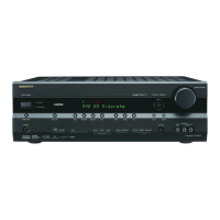
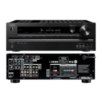
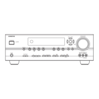
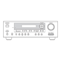
HT-R510
TERMINAL DESCRIPTION
MAIN MICROPROCESSOR
 Loading...