IC BLOCK DIAGRAMS AND TERMINAL DESCRIPTIONS-14
Q301 : CS42518 (8-ch Codec with S/PDIF Receiver)-3/4
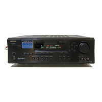
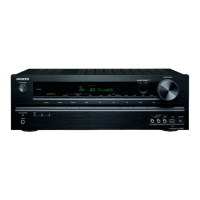
TX-SR504/504E/8450
TERMINAL DESCRIPTION(2/3)
Pin Name # Pin Description
AD0/CS 10 Address Bit 0 (I2C)/Control Port Chip Select (SPI) (INput) - AD0 is a chip address pin in I2C mode; CS
is the chip select signal in SPI mode.
INT 11 Interrupt (Ountput) - The CS42518 will generate an interrupt condition as per the Interrupt Mask register.
RST 12 Reset (Input) - The device enters a low power mode and all internal registers are reset to their default
settings when low.
AINR-
AINR+
13
14
Differential right Channel Analog Input (Input) - Signals are presented differentially to the delta-sigma
modulators via the AINR+/- pins.
AINL-
AINL+
15
16
Differential right Channel Analog Input (Input) - Signals are presented differentially to the delta-sigma
modulators via the AINR+/- pins.
VQ 17 Quiescent Voltage (Output) - Filter connection for internal quiescent reference voltage.
FILT+ 18 Positive Voltage Reference (Output) - Positive reference voltage for the internal sampling circuits.
REFGND 19 Reference Ground (Input) - Ground reference for the internal sampling circuits.
AOUTA1 +, -
AOUTB1 +, -
AOUTA2 +, -
AOUTB2 +, -
AOUTA3 +, -
AOUTB3 +, -
AOUTA4 +, -
AOUTB4 +, -
36, 37
35, 34
32, 33
31, 30
28, 29
27, 26
22, 23
21, 20
Differential Analog Output (Output) - The full-scale differential analog output level is specified in the
Analog Characteristics specification table.
VA
VARX
24
41
Analog Power (Input) - Positive power supply for the analog section.
AGND 25
40
Analog Ground (Input) - Ground reference. Should be connected to analog ground.
MUTEC 38 Mute Control (Output) - The Mute Control pin outputs high impedance following an initial power -on con-
dition or whenever the PDN bit is set to a "1", forcing the codec into power -down mode. The signal will
remain in a high impedance state as long as the part is in power-down mode. The Mute Control pin goes
to the selected "active" state during reset, muting, or if the master clock to left/right clock frequency ratio
is incorrect. This pin is intended to be used as a control for external mute circuits to prevent the clicks
and pops that can occur in any single supply system. The use of external mute circuits are not manda-
toy but may be desired for designs requiring the absolute minimum in extraneous clicks and pops.
LPFLT 39 PLL Loop Filer (Output) - An RC network should be connected between this pin and ground.
RXP7/GPO7
RXP6/GPO6
RXP5/GPO5
RXP4/GPO4
RXP3/GPO3
RXP2/GPO2
RXP1/GPO1
42
43
44
45
46
47
48
S/PDIF Receiver Input/ General Purpose Output (Input/ Output) - Receiver inputs for S/PDIF encoded
data. The CS42518 has an internal 8:2 multiplexer to select the active receiver port, according to the
Receiver Mode Control 2 resister. These pins can also be configured as general purpose output pins,
ADC Overflow indicators or Mute Control outputs according to the RXP/General Purpose Pin Control
resisters.
RXP0 49 S/PDIF Receiver Input (Input) - Dedicated receiver input for S/PDIF encoded data.
TXP 50 S/PDIF Transmitter Output (Output) - S/PDIF encoded data output, mapped directly from one of the
receiver inputs as indicated by the Receiver Mode Control 2 resister.
VLP 53 Serial Port Interface Power (Input) - Determines the required signal level for the serial port interfaces.
SAI_SDOUT 54
Serial Audio Interface Serial Data Output (Output) - Output for two's complement serial audio PCM
data from the S/PDIF incoming stream. This pin can also be configured to transmit the output of the inter-
nal and external ADCs.
RMCK 55 Recovered Master Clock (Output) - Recovered master clock output from the External Clock Reference
 Loading...