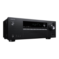
TX-8222
IC BLOCK DIAGRAMS AND DESCRIPTIONS
1
2
3
5
6
7
8
9
PROTECTOR
REGU-
LATOR
Vss
OUT1
OUT2
IN1 IN2 GND
Vcc Vref
TA7291S(Volume motor driver)
IN1
0
1
0
1
IN2 OUT1 OUT2
0 STOP
0 H L CW/CCW
1 L H CCW/CW
1 L L BRAKE
CCW: Counter-clockwise
CW: Clockwise
INPUT OUTPUT
MODE
S1
S2
S3
S4
S5
S6
S7
S8
S9
S10
S11
S1
S2
S3
S4
S5
S6
S7
S8
S9
S10
S11
VSS VDD
GND CK DATA STB
LEVEL SHIFTER+SHIFT REGISTER
CIRCUIT
(R-ch)
10bit
Latch
Circuit
(Same
as L-ch
Circuit)
(L-ch)
10bit
Latch
Circuit
2
3
4
5
6
7
8
9
10
11
12
27
26
25
24
23
22
21
20
19
18
17
13 14 15 16
1
28
TC9273CNG(Analog Switch Array)
Pin No. Symbol Description
1 Vss Negative power supply pin
13 GND Digital ground pin
28 VDD Positive power supply pin
2/27 S1
3/26 S2
4/25 S3
5/24 S4
6/23 S5
7/22 S6
8/21 S7
9/20 S8
10/19 S9
11/18 S10
12/17 S11
14 CK Clock input pin for data transfer.
15 DATA Serial data input pin for setting switches.
16 STB Strobe input pin for data writing.
Input/Output pins

 Loading...