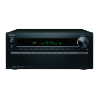
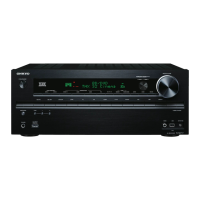
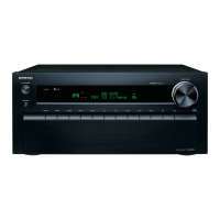
Do you have a question about the Onkyo TX-NR3010S and is the answer not in the manual?
Instructions for replacing fuses in the unit, emphasizing the use of same type and rating for safety.
Perform safety checks, including leakage current measurement, before releasing the unit to the customer.
Procedure to initialize the unit to factory settings by pressing specific buttons while powering on.
Steps to check the firmware version of the main microprocessor and DSPs by using the FL tube display.
Important notes on handling the power supply board, emphasizing high voltage safety and discharging capacitors.
Display mode for audio information to check operations of DSP and DIR for digital audio troubleshooting.
Explanation of the display contents in audio debug mode, including muting ports and input terminals.
Details of input formats used for listening mode transition, specifying source format and display information.
Information on sampling frequency for display and input, covering unknown, kHz, and MHz values.
Check for audio output status (Decode OK/NG) based on DSP detection.
Details of input formats for display, covering source format and specific codes like ANA, PCM, and DTS.
Overview of the content displayed in HDMI debug mode, including resolution display and standard resolutions.
A list of standard resolutions supported, showing various formats like 480i, 720p, 1080i, and VGA.
Shows how input resolution is displayed in HDMI debug mode for DVI, VGA, and no input signals.
Illustrates the display of output resolution in HDMI debug mode for various conditions like VSP, DVI, VGA, RSEN, EDID.
Shows the display of input resolution for 4K Upscaling, including various resolution formats.
Details the display of output resolution for 4K Upscaling, including resolution errors and EDID read status.
Illustrates the display of input resolution in HDMI debug mode, showing status for RSEN OFF, EDID READ NG, and Resolution Error.
Provides status information for HDMI input, including Input Mode, Input Color, and Deep Color.
Details the various 3D formats supported, such as Frame Packing, Field Alternative, and Side-by-Side.
Displays PC resolution information for input and output, including horizontal and vertical resolution.
Shows the display of input resolution for DVI, HDMI, and no input conditions.
Illustrates the display of output resolution for DVI and HDMI, including resolution through and EDID read status.
Confirms speaker relay operation, checking ON time after power is on and OFF time after power is off.
Checks voltage detection protectors by changing the state to TEST-4-24 and verifying sequential displays.
Verifies current detection protectors by connecting loads and checking relay response.
Confirms HDMI main output OSD operation, checking setup menu and screen display at power on.
Confirms selector muting, audio/video selector operation, and firmware combination check.
Checks cooling fan operation at different states (no input, slow speed, fast speed).
Confirms video output signal against input signals, covering composite video and component signals.
Details test modes for model, destination, and FL display, including segment lit tests and destination display.
Describes test modes for operation, including push button combinations and test number sequences.
Continues the description of test modes for operation, detailing input/output signals and speaker relay checks.
Details test modes for operation using auto measurement, covering DSP output channels and relay checks.
Continues test mode operations, specifying input selectors, Zone 2 settings, and I2S/SPDIF signal confirmation.
Describes the cooling fan circuit, conditions for operation, hysteresis control, and how to check its function.
Diagram illustrating the audio block structure, showing signal flow from inputs to outputs and DSP sections.
Diagram showing the video block structure, detailing signal paths for component, composite, and D4 interfaces.
Diagram outlining the HDMI block structure, illustrating signal flow for HDMI inputs, processors, and outputs.
Diagram detailing the digital audio block, showing signal paths for various digital inputs and DSP processing.
Schematic for the first stage of the amplifier section, focusing on voltage amplification circuits.
Schematic for the final stage of the amplifier section, illustrating power supply and output circuits.
Schematic of the third amplifier stage, covering power supply, protection circuits, and thermal sensors.
Schematic for the Analog Signal Processing (ASP) section, covering audio inputs and DSP interface.
Schematic for the second Analog Signal Processing (ASP) section, detailing DSP and audio signal routing.
Schematic illustrating the analog video signal processing, including input and output paths.
Schematic of the Analog Front End (AFE) tuner section, detailing RF and antenna connections.
Schematic illustrating the Digital-to-Analog Converter (DAC) section, showing signal processing for audio channels.
Schematic for the digital section, covering signal processing for HDMI, I2S, and SPDIF interfaces.
Schematic of the digital power supply, showing voltage regulation and distribution for various digital components.
Schematic detailing the Central Processing Unit (CPU) section, including memory interfaces and control signals.
Schematic for the display section, covering vacuum fluorescent display (VFD) and selector LEDs.
Schematic illustrating the speaker terminal connections, including relay circuits and amplifier output routing.
Schematic of the primary power supply, detailing switching PS, transformers, and fuse protection.
Schematic for the first HDMI section, covering HDMI sub output and related signal paths.
Schematic illustrating the HDMI input 2 section, detailing connections to the SPARTA2 and VMPU sections.
Schematic for the HDMI Receiver (RX) and Decoder section, showing connections to ADV7844 and VMPU.
Schematic detailing the HDMI Main section, showing connections to HQV, VMPU, and HDMI RX/Encoder parts.
Schematic for the HQV and Connector section, detailing connections to HDMI RX, VMPU, and DSP sections.
Schematic of the HDMI Main section, illustrating connections to VMPU, Encoder, and Power Supply.
Schematic for the 1st DSP memory section, showing connections to the HDMI PC board and other DSP modules.
Schematic detailing the DSP, Audio, and GPIO section, including connections to AFE and other processors.
Schematic for the Ethernet, USB, and GPIO section, showing connections to the HDMI PC board and ARM processor.
Schematic for the 2nd DSP section, illustrating connections to memory, AFE, and other DSP modules.
Schematic detailing the front USB and USB section, showing connections to the HDMI PC board and other controllers.
| Channels | 9.2 |
|---|---|
| HDMI Inputs | 8 |
| Network Capability | Yes |
| Room Calibration | Audyssey MultEQ XT32 |
| THX Certified | THX Ultra2 Plus |
| 4K Passthrough | Yes |
| 3D Support | Yes |
| AirPlay | Yes |
| Phono Input | Yes |
| DLNA | Yes |
| Wi-Fi | No |
| Bluetooth | No |
| Dimensions (W x H x D) | 435 x 198.5 x 463.5 mm |
| HDMI Outputs | 2 |
| Audio Formats Supported | Dolby TrueHD, DTS-HD Master Audio, Dolby Digital Plus, DTS-HD High Resolution Audio, Dolby Digital, DTS |
| Streaming Services | vTuner, Pandora, Spotify |
| THD | 0.08% |
| Frequency Response | 5Hz-100kHz |
| Input Sensitivity and Impedance | 200mV/47k ohms |
| Signal-to-Noise Ratio | 110dB |
| Digital Audio Inputs/Outputs | 3 Optical Inputs, 3 Coaxial Inputs |
| USB Port | 1 (front) |
| Weight | 55.1 lbs (25 kg) |
