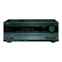
TX-SR702/E
IC BLOCK DIAGRAMS AND DESCRIPTIONS
ADV7183AKST(Multiformat SDTV Video Decoder)
Pin Function Descriptions
Pin No. Mnemonic Type Function
3, 9, 14, 31, 71 DGND G
Digital Ground.
39, 40, 47, 53, 56 AGND G
Analog Ground.
4, 15 DVDDIO P Digital I/O Supply Voltage (3.3 V)
.
10, 30, 72 DVDD P
Digital Core Supply Voltage (1.8 V).
50 AVDD P Analog Supply Voltage (3.3 V).
38 PVDD P PLL Supply Volt
age (1.8 V).
41…46, 57…62 AIN1…AIN12 I
Analog Video Input Channels.
11, 13, 16…18, 25,
34, 35, 63, 65, 69,
70, 77, 78
NC
No Connect Pins.
5…8, 19…24,
32, 33, 73…76
P0…P15 O Video Pixe
l Output Port.
2 HS O HS is a horizontal synchronizatio
n output signal.
1 VS O VS is a vertical synchronization
output signal.
80 FIELD O FIELD is a field synchronization
output signal.
67 SDA I/O I
2
C Port Serial Data Input/Output Pin.
68 SCLK I I
2
C Port Serial Clock Input (Max Clock Rate of 400 kHz).
66 ALSB I
This pin selects the I
2
C address for the ADV7183A. ALSB set to Logic 0 sets the address
for a write as 0x40; for ALSB set to logic high, the ad d ress selected
is 0x42.
64
RESET
I
System Reset Input, Active Low. A minimum low reset pulse width of 5 ms is required to
reset the ADV71
83A circuitry.
27 LLC1 O
This is a line- locked output clock for the pixel data output by the ADV7183A. Nominally
27 MHz, but varies up or down according to video line le
ngth.
26 LLC2 O
This is a divide-by-2 version of the LLC1 output clock for the pixel data output by the
ADV7183A. Nominally 13.5 MH z, but varies up or
down according to video line length.
29 XTAL I
This is the input pin for the 27 MHz crystal, or can be overdriven by an external 3. .3 V,
27 MHz clock oscillator source. In crystal mode,
the crystal must be a fundamental crystal.
28 XTAL1 O
This pin should be connected to the 27 MHz crystal or left as a no connect if an external
3.3 V, 27 MHz clock oscillator source is used to clock the ADV7183A. In crystal mode,
the crystal must be a fundamental crystal.
36
PWRDN
I
A logic low on this pin places the ADV7183A in a power-down mode. Refer to the I2C
Control Register Map for more options on power-down modes for the ADV7183
A.
79
OE
I
When set to a logic low, OE enables the pixel output bus, P15…P0 of the ADV7183A. A logic
high on the OE pin places Pins P15…P0, HS, VS, SFL/SYNC_OUT into a high impedance state.
37 ELPF I
The recommended external loop filter must be connected to this ELPF pin, as shown in
Figure 42.
12 SFL O
Subcarrier Frequency Lock. This pin contain s a se rial output stream that can be used to lock
the subcarrier frequency when this decoder is connected to any Analog Devices, Inc. digital
video encoder.
51 REFOUT O
Internal Voltage Reference Output. Refer to Figure 42 for a recommended capa citor
network for this
pin.
52 CML O
The CML pin is a common-mode level for the internal ADCs. Refer to Figure 42 for a
recommended capacitor networ
k for this pin.
48, 49 CAPY1,
CAPY2
I
ADC s Capacitor Network. Refer to Figure 42 for a recommended capacitor network for
this pin.
54, 55 CAPC1,
CAPC2
I
ADC s Capacitor Network. Refer to Figure 42 for a recommended capacitor network for
this pin.
 Loading...