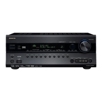
Do you have a question about the Onkyo TX-SR707 and is the answer not in the manual?
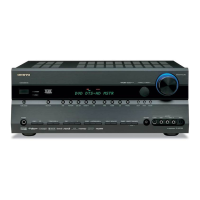
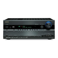
Definitions for model abbreviations used in exploded views.
Key for safety marks, part status, and model variations.
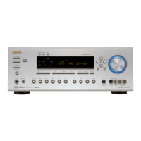
| Impedance | 4 Ω |
|---|---|
| Frequency range | 5 - 100000 Hz |
| Signal-to-Noise Ratio (SNR) | 106 dB |
| Total Harmonic Distortion (THD) | 0.08 % |
| AM band range | 522 - 1611 kHz |
| FM band range | 87.5 - 108 MHz |
| Radio Data System (RDS) | Yes |
| Package depth | 570 mm |
| Package width | 469 mm |
| Package height | 298 mm |
| Dimensions (WxDxH) | 435 x 175 x 379 mm |
| Power requirements | AC 220-240 V, 50/60 Hz |
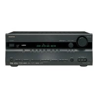
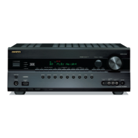
| Product color | Black |
| Package weight | 16800 g |
| Power consumption (typical) | 600 W |
| Weight | 12600 g |
|---|