8.2. GENERAL BLOCK DIAGRAM
The control section will be explained as shown in the block diagram.
1. ASIC (IC1)
Composed mainly of an address decoder, modem control section, CPU and RTC.
Controls the general FAX operations.
Controls the operation panel I/F.
Controls the thermal head I/F and CIS I/F.
Executes image processing.
TAM monitor and the H/S volume.
I/O ports
2. ROM (IC2)
Contains all of the program instructions for unit operations.
3. Static RAM (IC4)
This memory is used mainly for the parameter working storage area.
4. MODEM (IC5)
Modem for the FAX.
5. Read Section
Contact Image Sensor (CIS) to read transmitting documents.
6. Thermal Head
Contains heating elements for dot matrix image printing.
7. Motor driver (IC7)
Drives the motor.
8. Analog board
Composed of an ITS circuit and NCU circuit.
9. Sensor Section
Composed of a document sensor, recording paper sensor, motor position sensors, read position sensor.
10. Power supply switching board section
Supplies +5V and +24V to the unit.
104
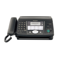
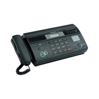
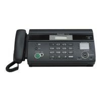
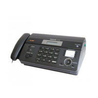
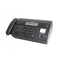
KX-FT901CX-B / KX-FT903CX-B / KX-FT901CX-W / KX-FT903CX-W / KX-FT901CX-S / KX-FT903CX-S
 Loading...