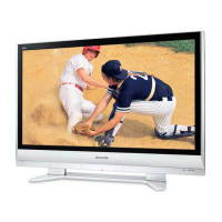
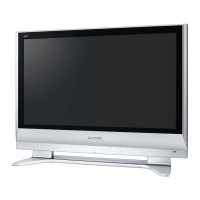
Do you have a question about the Panasonic TH-C42FD18 and is the answer not in the manual?
Guidelines for conducting repairs and servicing safely.
Procedure to check leakage current when the unit is unplugged.
Procedure to check leakage current when the unit is powered.
Techniques to prevent damage to sensitive electronic components from static discharge.
Instructions for accessing the service mode using remote control commands.
Details of adjustable parameters within the service mode, like contrast, color, and WB.
Steps to access the service tool mode from the service mode menu.
Procedures for checking IIC bus lines for proper communication.
Information about Power LED blinking patterns to diagnose issues.
Steps to access the IIC bus line check function from the TV.
Initial checks for no power indication based on the power LED status.
General procedure for adjusting driver section voltages.
Preparation for driver setup, including inputting a white signal and setting picture controls.
Specific items and preparations needed before starting driver setup.
Adjusting driver section voltages using a multimeter, referring to panel data.
Procedure for adjusting initialization pulse using an oscilloscope.
Cautionary note regarding PCB exchange, specifically waiting for capacitor discharge.
Adjusting voltages with a multimeter after replacing PCBs.
Procedure for adjusting white balance using a color analyzer and specific patterns.
Schematic diagram for the P-Board, part 1 of 2.
Schematic diagram for the P-Board, part 2 of 2.
Schematic diagram for the A-Board, part 1 of 12.
Schematic diagram for the A-Board, part 2 of 12, showing DDR interface.
Schematic diagram for the A-Board, part 3 of 12, detailing digital signal processing.
Schematic diagram for the A-Board, part 4 of 12, showing power supply circuitry.
Schematic diagram for the A-Board, part 5 of 12, showing connector and AV switch functions.
Schematic diagram for the A-Board, part 6 of 12, detailing audio amplifier and control signals.
Schematic diagram for the A-Board, part 7 of 12, showing GenX5 microcontroller and EEPROM connections.
Schematic diagram for the A-Board, part 8 of 12, illustrating LVDS transmitter and driver ICs.
Schematic diagram for the A-Board, part 9 of 12, detailing HDMI interface and multiplexer functions.
Schematic diagram for the A-Board, part 10 of 12, showing HDMI interface and signal routing.
Schematic diagram for the A-Board, part 11 of 12, focusing on the front-end tuner and tuner control.
Schematic diagram for the A-Board, part 12 of 12, illustrating LVDS transmitter connections.
Schematic diagram for the D-Board, part 1 of 6, showing various driver ICs and connections.
Schematic diagram for the D-Board, part 2 of 6, detailing FPGA and other interface connections.
Schematic diagram for the D-Board, part 3 of 6, showing driver ICs and their connections.
Schematic diagram for the D-Board, part 4 of 6, illustrating DDR memory and other interface connections.
Schematic diagram for the D-Board, part 5 of 6, showing driver ICs and connections.
Schematic diagram for the D-Board, part 6 of 6, showing driver ICs and connections.
Schematic diagram for the C1-Board, part 1 of 3, showing driver ICs and connections.

