EasyManua.ls Logo

Panasonic TH-L32C53T

Panasonic TH-L32C53T
71 pages
To Next Page IconTo Next Page
Loading...
© Panasonic Corporation 2012. Unauthorized
copying and distribution is a violation of law.
ORDER NO. MTV1207163CE
LCD TV
Model No. TH-L32C53T
Chassis: KM17
Destination: THAILAND
TABLE OF CONTENTS
PAGE PAGE
1 Safety Precautions----------------------------------------------- 3
1.1. General Guidelines---------------------------------------- 3
1.1.1. Leakage Current Cold Check---------------------- 3
1.1.2. Leakage Current Hot Check (See Figure
1.) --------------------------------------------------------- 3
2 Warning -------------------------------------------------------------- 4
2.1. Prevention of Electrostatic Discharge (ESD)
to Electrostatically Sensitive (ES) Devices---------- 4
2.2. About lead free solder (PbF)---------------------------- 5
3 Service Navigation ----------------------------------------------- 6
3.1. Service Hint ------------------------------------------------- 6
4 Specifications ----------------------------------------------------- 7
5 Service Mode ------------------------------------------------------ 9
5.1. How to enter into Service Mode ----------------------- 9
5.1.1. Contents of adjustment mode --------------------- 9
5.1.2. How to exit---------------------------------------------- 9
5.2. SRV-TOOL -------------------------------------------------10
5.2.1. How to access ----------------------------------------10
5.2.2. Display of SOS History -----------------------------10
5.2.3. POWER ON TIME/COUNT -----------------------10
5.2.4. Exit ------------------------------------------------------ 10
5.2.5. Self Check (Device) -------------------------------- 11
5.2.6. Hotel Mode Adjustment---------------------------- 11
5.2.7. Hotel Mode-------------------------------------------- 11
6 Troubleshooting Guide --------------------------------------- 12
6.1. Check of the IIC bus lines------------------------------ 12
6.1.1. How to access --------------------------------------- 12
6.1.2. Exit ------------------------------------------------------ 12
6.1.3. Screen display --------------------------------------- 12
6.2. Power LED Blinking timing chart --------------------- 13
6.3. No Power--------------------------------------------------- 13
7 Disassembly and Assembly Instructions--------------- 14
7.1. Control Button Assembly------------------------------- 14
7.2. Speaker Unit Installation ------------------------------- 16
7.3. LCD Panel Assembly ----------------------------------- 18
7.4. LCD Panel Fixing & Handling Method -------------- 20
7.5. LED Panel Assembly------------------------------------ 21
7.6. LVDS & Barrier Assembly------------------------------ 22
7.7. Metal Part Assembly ------------------------------------ 24
7.8. Screws Fixing --------------------------------------------- 25

Table of Contents

Question and Answer IconNeed help?

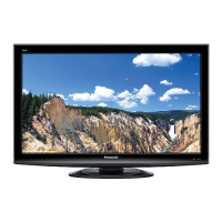
Do you have a question about the Panasonic TH-L32C53T and is the answer not in the manual?

Panasonic TH-L32C53T Specifications

General IconGeneral
BrandPanasonic
ModelTH-L32C53T
CategoryLCD TV
LanguageEnglish

Summary

Safety Precautions

General Guidelines

Basic rules for safe and proper servicing procedures.

Leakage Current Checks

Procedures for checking AC leakage current (cold and hot).

Electrostatic Discharge (ESD) Prevention

Techniques to prevent damage from static electricity to sensitive components.

Lead Free Solder (PbF) Handling

Guidance on using and handling lead-free solder during repairs.

Service Navigation

Service Hint

Provides hints and board identification for service navigation.

Specifications

Receiving Systems and Channels

Details about supported TV broadcast reception systems and channel ranges.

Operating Conditions and Terminals

Specifies environmental operating conditions and available input/output connection terminals.

Service Mode

Entering and Exiting Service Mode

Instructions on how to access and exit the TV's service mode.

Adjustment Mode Contents

Lists parameters and sample data available for adjustment within the service mode.

SRV-TOOL Functions

Details on using the SRV-TOOL for diagnostics, history, and time/count display.

Hotel Mode Configuration

How to enable, adjust, and understand hotel mode settings to restrict TV functions.

Self Check (Device)

Procedure to perform a self-check of the TV's internal devices.

Troubleshooting Guide

IIC Bus Line Check

Steps to access and interpret the IIC bus line self-check screen.

Power LED Blinking Chart

Identifies common faults by interpreting power LED blinking patterns.

No Power Troubleshooting

Diagnostic flowchart for troubleshooting power-related issues based on LED status.

Disassembly and Assembly Instructions

Control Button Assembly

Step-by-step guide for disassembling and reassembling the control button assembly.

Speaker Unit Installation

Instructions for correctly installing the left and right side speaker units.

LCD Panel Assembly

Detailed procedure for assembling the LCD panel into the TV chassis.

LCD Panel Fixing & Handling

Precautions and methods for safely fixing and handling the LCD panel to prevent damage.

LED Panel Assembly

Steps for assembling the LED panel, including bracket and wire connections.

LVDS & Barrier Assembly

Guide for fixing the LVDS barrier and cable connections to the LCD panel.

Metal Part Assembly

Instructions for assembling metal components like bottom covers and VESA mounts.

Screws Fixing

Details on the types and torque specifications for screws used during assembly.

PCB Installation

Steps for installing various PCBs (P-board, A-board) and connecting panel lead wires.

Back Cover Installation

Procedure for installing the back cover, model nameplate, and AC cord.

Measurements and Adjustments

A-board Voltage Chart

Specifies test points and expected voltages for the A-board during measurement.

IP-board Voltage Chart

Specifies test points and expected voltages for the IP-board during measurement.

White Balance Adjustment Target

Defines target values for white balance adjustment under different ambient temperature conditions.

Block Diagram

Main Block Diagram

Overview of the TV's main functional blocks and their interconnections.

Wiring Connection Diagram

Wire Dressing

Illustrates the correct routing and placement of internal wires and cables.

Schematic Diagram

Schematic Diagram Notes

Explains symbols, units, and measurement conditions used in schematic diagrams.

A-Board (116) Schematic Diagram

Circuit diagram detailing the IIC bus and related components on the A-board.

A-Board (216) Schematic Diagram

Circuit diagram showing HDMI, ARC, Tuner, and Audio AMP connections on the A-board.

A-Board (316) Schematic Diagram

Circuit diagram for AVSW, Monitor Out, and Video/Audio In sections of the A-board.

A-Board (416) Schematic Diagram

Circuit diagram for Initial Setup, STM, and Peaks ports on the A-board.

A-Board (516) Schematic Diagram

Circuit diagram focusing on the backlight control section of the A-board.

A-Board (616) Schematic Diagram

Circuit diagram for LVDS interface and T-CON related circuits on the A-board.

A-Board (716) Schematic Diagram

Circuit diagram for Power Key, SOS, Power Detect, and Analog ASIC on the A-board.

A-Board (816) Schematic Diagram

Circuit diagram for terminal connections (HDMI, USB) and overall set configuration on the A-board.

A-Board (916) Schematic Diagram

Circuit diagram for common NAND, SPC, EEPROM, and JTAG interfaces on the A-board.

A-Board (1016) Schematic Diagram

Circuit diagram for LAN, SD, and USB interfaces on the A-board.

A-Board (1116) Schematic Diagram

Circuit diagram illustrating various power supply circuits (STB5V, SUB1.8V, etc.) on the A-board.

A-Board (1216) Schematic Diagram

Circuit diagram detailing various I/O ports, power controls, and interface signals on the A-board.

A-Board (1316) Schematic Diagram

Circuit diagram showing specific power supply rails (SUB1.2V, SUB1.8V) and related components on the A-board.

A-Board (1416) Schematic Diagram

Circuit diagram for DCDC converters (SUB1.2V, SUB1.5V) and related control logic on the A-board.

A-Board (1516) Schematic Diagram

Circuit diagram for DDR memory interface (CHO, CH1) and associated signals on the A-board.

A-Board (1616) Schematic Diagram

Circuit diagram for various reference voltages and destination-specific signals on the A-board.

GK-Board Schematic Diagram

Circuit diagram for the GK-board, detailing control buttons and key scan signals.

K-Board Schematic Diagram

Circuit diagram for the K-board, including RM receiver and power LED circuitry.

IP-Board Schematic Diagram

Circuit diagram for the IP-board, illustrating power supply and inverter functions.

Printed Circuit Board

A-BOARD (Top Component Side)

Layout and component placement for the top side of the A-board.

A-BOARD (Bottom Component Side)

Layout and component placement for the bottom side of the A-board.

GK-BOARD

Layout and component placement for the GK-board.

K-BOARD

Layout and component placement for the K-board.

IP-BOARD

Layout and component placement for the IP-board.

Exploded View and Replacement Parts List

Exploded View and Mechanical Parts List

Visual representation of mechanical parts and their list for replacement.

Electrical Replacement Parts List Notes

Explains notes and abbreviations related to the electrical replacement parts list.

Related product manuals