16
HUDSON 8
DDC Instructions
Pin No. Description
1 T.M.D.S. data2-
2 T.M.D.S. data2+
3 T.M.D.S. data2 shield
4 No Connect
5 No Connect
6 DDC clock
7 DDC data
8 No Connect
9 T.M.D.S. data1-
10 T.M.D.S. data1+
11 T.M.D.S. data1 shield
12 No Connect
13 No Connect
14 +5V Power
15 Ground (for +5V) - Cable detect
16 Hot plug detect
17 T.M.D.S. data0-
18 T.M.D.S. data0+
19 T.M.D.S. data0 shield
20 No Connect
21 No Connect
22 T.M.D.S clock shield
23 T.M.D.S. clock+
24 T.M.D.S. clock-
To Monitor
D-sub/DVI cable
DC 8~12V
To Printer port
Power
indicator
To Monitor
D-sub cable
DC 8~12V
To Printer port
Power
indicator
General
DDC Data Re-programming
In case the DDC data memory IC or main EEPROM which storage all
factory settings were replaced due to a defect, the serial numbers have
to be re-programmed"Analog DDC IC, & EEPROM".
It is advised to re-soldered DDC IC and main EEPROM from the old
board onto the new board if circuit board have been replaced, in this case
the DDC data does not need to be re-programmed.
Additional information
Additional information about DDC (Display Data Channel) may be
obtained from Video Electronics Standards Association (VESA).
Extended Display Identification Data(EDID) information may be also
obtained from VESA.
1. An i486 (or above) personal computer or compatible.
2. Microsoft operation system Windows 95/98 .
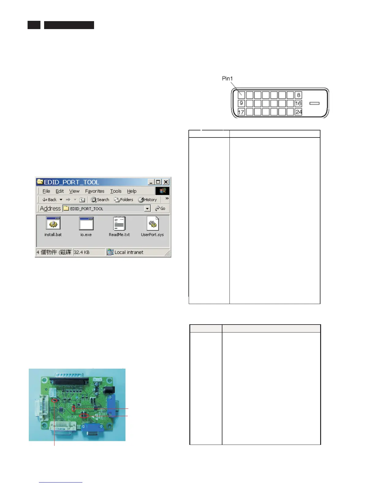
Y o Install the EDID_PORT_Tool under Win2000/XP . As
Fig. 1 .
A. Copy the "UserPort.sys" to C:\WINNT\system32\drivers(win2000)
C:\WINDOWS\system32\drivers(winXP)
B. Running " io.exe" everytime, Before you start to programming
edid data .
4. DDC 2BI-ISP TOOL:
Inclusion :
A. DDC2BI-ISP TOOL(3138 106 10396) x1 (as Fig. 2)
B. Printer cable x1
c. (D-Sub) to (D-Sub) cable x2
D. D-SUB to DVI cable X1
Note: The EDID46.EXE is a windows-based program, which cannot
be run in MS-DOS.
System and equipment requirements
ou have t
3. EDID45.exe program .
Fig. 2Fig. 2
Fig. 1Fig. 1
Pin Assignment
The digital only connector contains 24 signal contacts organized in
three rows of eight contacts. Signal pin assignments are listed in the
following table:
Fig. 3Fig. 3
Fig. 4Fig. 4
Input analog D-sub connector pin assignment
PIN No. SIGNAL
1 Red video input
2 Green video input / sync on green
3 Blue video input
4GND
5 GND--Cable detect
6 Red video GND
7 Green video GND
8 Blue video GND
9 DDC +3.3V or +5V
10 Logic GND
11 GND
12 Serial data line (SDA)
13 H-sync / H+V
14 V-sync
15 Data clock line (SCL)
Jumper at VGA_5V position
Jumper at VGA position
Jumper at NORMAL position



 To Next Page