8-1 8-1
AC POWER & DISPLAY & KEY
BOARD
TABLE OF CONTENTS
Internal IC Diagram ......................................................... 8-1
Layout Diagram - AC Power Board ................................. 8-2
Circuit Diagram - AC Power Board.................................. 8-3
Layout Diagram - AC Socket Board ................................ 8-4
Layout Diagram - Door Moter Board ............................... 8-4
Layout Diagram - RC Board ............................................ 8-4
Display Board .................................................................. 8-5
Key Board ........................................................................ 8-6
Speaker & Ant Board ....................................................... 8-7
Electrical Parts List .......................................................... 8-8
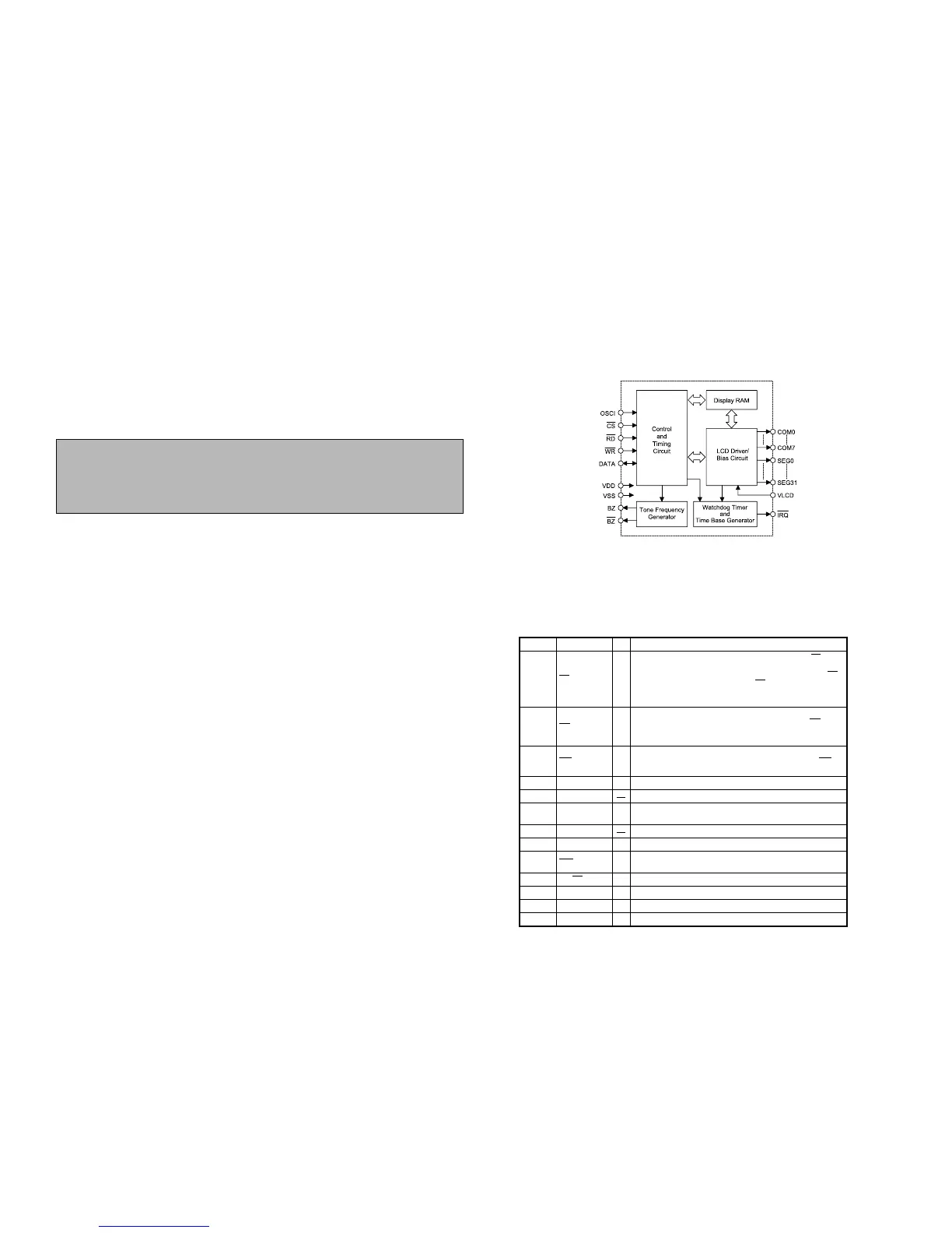
Block Diagram
IC BLOCK DIAGRAM - LCD DRIVER
HT1622
PIN DESCRIPTION - LCD DRIVER
HT1622
Pad Description
noitpircseDO/IemaNdaP.oNdaP
1CS
I
Chip selection input withPull-high resistor. When the CS is logic
high, the data and command read from or written to the HT1622
are disabled. The serial interface circuit is also reset. But if CS is
at logic low level and is input to the CS pad, the data and com
-
mand transmission between the host controller and the HT1622
are all enabled.
2RD I
READ clock input with Pull-high resistor. Data in the RAM of
the HT1622 are clocked out on the rising edge of the RD signal.
The clocked out data will appear on the data line. The host con -
troller can use the next fallingedge tolatchthe clocked out data.
3WR I
WRITE clock input with Pull-high resistor. Data on the DATA
line are latched into the HT1622 on therising edge of the WR sig-
nal.
4DATAI/O Serial data input/output with Pull-high resistor
5 VSS
Negative power supply, ground
6 OSCI I
If the system clock comes from an external clock source, the ex -
ternal clock source should be connected to the OSCI pad.
7 VDD Positive power supply
8 VLCD I LCD operating voltage input pad
9 IRQ
O
Time base or Watchdog Timer overflow flag, NMOS open drain
output
10, 11 BZ, BZ O 2kHz or 4kHz tone frequency output pair
12~14 T1~T3 I Not connected
15~22 COM0~COM7 O LCD common outputs
23~54 SEG0~SEG31 O LCD segment outputs