SECTION 2 - TECHNICAL DESCRIPTION
Page 2.1
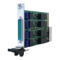
PXI/PXIe LVDT/RVDT/Resolver Simulator Module 41/43-670
pickering
SECTION 2 - TECHNICAL DESCRIPTION
FUNCTIONAL DESCRIPTION
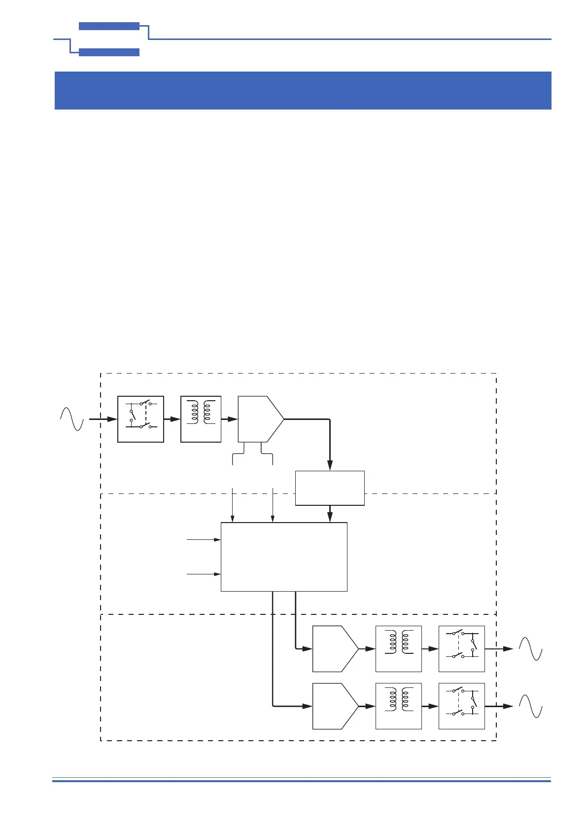
Figure 2.1 - LVDT Simulator Module 41/43-670: Functional Diagram For One Bank
Input Isolation
Transformer
Output Isolation
Transformer
Output Isolation
Transformer
Input Switching
Output Switching
Output Switching
DAC
Output A
DAC
Output B
Sampling
ADC
FIFO Circular
Buffer
Real Time Digital
Signal Processor
Measured
Frequency
Value
Measured
Input Level
Value
Phase & Amplitude
Correction
Calibration Data
Control
Requests
Input
Output
Signal Processing
A
B
In
The 41/43-670 module can be supplied with between one and four banks which can be specied for the simulation
of Linear Variable Differential Transformers (LVDT), Rotary Variable Differential Transformers (RVDT) or Resolvers.
Five ranges of excitation input are available between 1.8V and 38V and ve output ranges between 1.8V and 31V.
The input for the bank corresponds to the excitation input for the LVDT/RVDT. It is routed through a switching
network and isolation transformer before being sampled by an ADC. The input switching can be used to simulate
open and short circuit fault conditions as well as allowing the input signal to be routed to other banks. The digital
representation of the input is stored in a circular buffer where it is read by the Signal Processor.
Based on stored calibration data, the Signal Processor performs correction on the input signal to ensure that the
phase and amplitude are consistent throughout the specied input range of the channel. The circular buffer can also
be loaded with internally generated data therefore allowing the simulator to operate without an external input signal.
The input signal data is used by the Signal Processor as the reference for the generation of the outputs. Control
requests enable the signal level to be varied between the A and B outputs to simulate 5/6-wire LVDTs, or A and B
can be set as differential outputs, each independently simulating a 4-wire LVDT. As well as simulating the normal
operation of an LVDT/RVDT, the outputs can be set with amplitude and phase difference to represent fault conditions.
The outputs from the Signal Processor are converted by DACs into A and B analog signals and are fed to the user
connector via isolation transformers and switching networks. The switching can be used to simulate open and short
circuit fault conditions. A functional diagram for one bank of the simulator is shown in Figure 2.1