SECTION 1 - TECHNICAL SPECIFICATION
Page 1.1
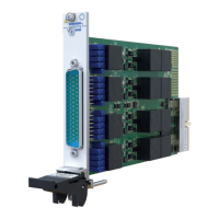
PXI/PXIe LVDT/RVDT/Resolver Simulator Module 41/43-670
pickering
SECTION 1 - TECHNICAL SPECIFICATION
pickeringtest.com
PXI/PXIe LVDT/RVDT/Resolver Simulator Module 41/43-670
ISSUE 2.3 OCT 2022
y Available as PXI or PXIe Modules
y Up to 4 Channels of 5/6-Wire LVDT/RVDT or Resolver,
or 8 Channels of 4-Wire LVDT/RVDT Simulation
y Input & Output Isolation Transformers
y Measurement & Display of Each Input Frequency
& Amplitude
y Wide Operational Frequency Band
y External or Internal Excitation
y Independent or Shared Excitation Signal to Each Channel
y Programmable phase delay
y Open & Short Circuit Simulation on Inputs & Outputs
y VISA, IVI & Kernel Drivers Supplied for
Windows Including Soft Front Panel
y PXI Version Supported by PXI or LXI Ethernet Chassis
y Customization Available
y 3 Year Warranty
The 41-670 (PXI) and 43-670 (PXIe) are ideal for the simulation
of variable differential transformers (VDT), both linear (LVDT)
and rotary (RVDT) types as well as resolvers. Available with up
to four banks, each bank is capable of simulating the output of
a single 5 or 6-wire VDT or resolver, or dual 4-wire utilising a
shared excitation signal. This allows the module to simulate up to
4 channels of 5 or 6-wire, or 8 channels of 4-wire.
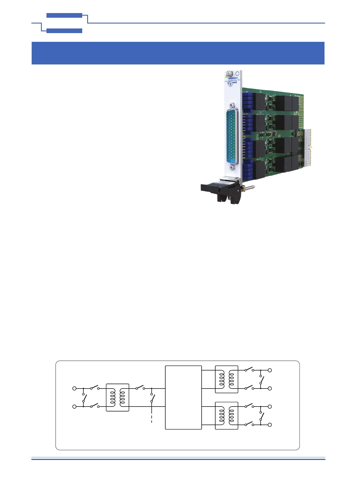
Each VDT bank has an independent excitation input, as well as
the ability to use an internally generated excitation signal. The
module also has the ability to take a single input and distribute
to all banks, reducing the load on the source and easing cabling.
Due to the use of transformers, each input and output is
galvanically isolated.
The 41/43-670 is designed for a wide band of excitation
frequencies, with 300 Hz to 20 kHz as standard, while also offering
input voltages up to 38 V and output voltages up to 31 V. Each
excitation input frequency and amplitude can also be
independently read back.
The phase relationship between the input and output signals is
automatically adjusted to lag one cycle, the result of which means
the phase delay can be negated. In applications where this is not
acceptable, one of the outputs can be used to propagate the input
signal resulting in an in phase signal with the output which can
then be used for demodulation.
With the addition of built in relays, the 41/43-670 can also provide
short or open circuits for each channel’s inputs and outputs,
reducing the need for external switching for fault insertion
requirements. The programmable phase delay can also be used for
simulating imperfect sensors and cabling, artificially offsetting a
single or multiple outputs.
The output amplitude is programmed using a number of options,
these include Vsum and Vdiff when operating in 5/6 wire,
percentage displacement and independent voltage outputs. Vsum
can be set as an absolute value or relative to the input amplitude.
Phase relationship is controlled via a programmable propagation
delay.
Additionally, the module can be programmed with an actuator
response, meaning rather than going from one position to the next
directly, it can change at a constant rate defined by the user.
Functional Diagram for One Bank of the 41/43-670 LVDT/RVDT/Resolver Simulator
Signal
Processing
In 1
Out 1A
Out 1B
To Next
Channel