Page 4.2
SECTION 4 - PROGRAMMING GUIDE
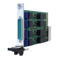
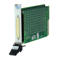
PXI/PXIe LVDT/RVDT/Resolver Simulator Module 41/43-670
pickering
USING THE SIMULATOR MODULE
41/43-670 LVDT Simulator Overview
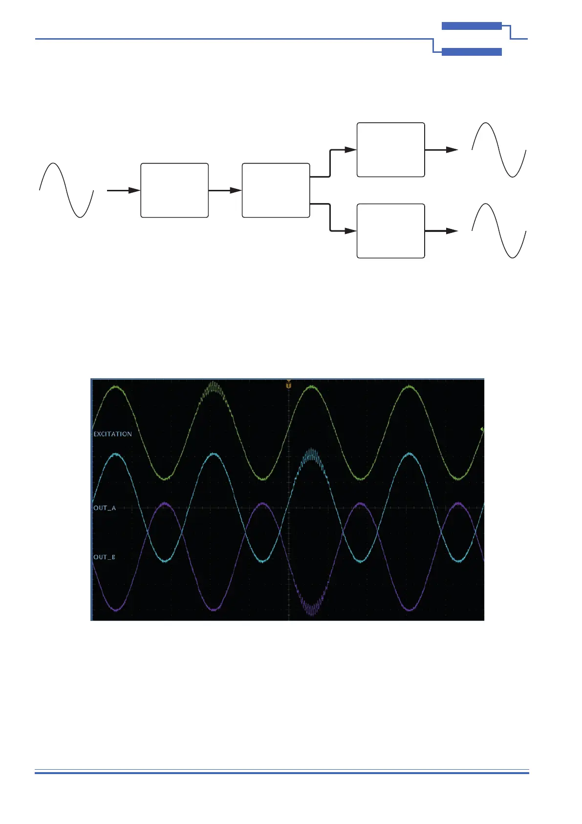
The LVDT Simulator continually samples the excitation input signal at 1.8MHz into a FIFO buffer, the output signal
is automatically synchronised to align its phase to the input phase, this allows adjustment either way from the
internal buffer in 555ns intervals to simulate phase offsets. As the sample frequency remains constant for lower input
frequencies it will have more points. The output waveforms are processed in real time to generate the outputs based
on the required conguration to simulate a wide range of LVDT applications.
By design, glitches and noise on the input waveform will be translated to the output, the output will be a real-world
output waveform rather than a perfectly synthesized one, it should however be noted that the output waveform will
always be exactly one cycle behind the input signal.
Sampling
ADC
Output B
DAC
Output A
DAC
LVDT
Simulator
Figure 4.1 - Example Input & Output Waveforms for the LVDT Simulator