Do you have a question about the Pioneer DJM-400 and is the answer not in the manual?
General safety precautions for continued protection of customer and service technician.
Special safety characteristics of electrical and mechanical parts identified by marking.
Details on power source, consumption, operating conditions, weight, and dimensions.
Specifications for sampling rate, converters, frequency response, S/N ratio, distortion, and levels.
List of input/output connectors including RCA, phone, and mini-phone jacks.
List of included accessories such as operating instructions and power cord.
Exploded view and parts list for the packing section of the unit.
Exploded view detailing external parts and their assembly.
Exploded view of the control panel components and their arrangement.
Overview of the unit's block diagram, showing major functional modules.
Detailed overall block diagram illustrating the main signal paths and component interactions.
Block diagram focusing on the CPU and DSP functions and their interconnections.
Diagram illustrating the wiring connections between major assemblies and components.
Detailed schematic diagram of the main assembly, part 1 of 3.
Detailed schematic diagram of the main assembly, part 2 of 3.
Detailed schematic diagram of the main assembly, part 3 of 3.
Schematic diagram of the Jack Assembly, part 1 of 4.
Schematic diagram of the Jack Assembly, part 2 of 4.
Schematic diagram of the Jack Assembly, part 3 of 4.
Schematic diagrams for the Jack Assembly (part 4) and Headphone Assembly.
Schematic diagram of the Microphone Assembly and its input selectors.
Schematic diagram of the power transformer and input voltage selection.
Schematic diagrams for the VR/SW Assembly (part 1) and CHRV Assembly.
Schematic diagram of the VR/SW Assembly, part 2 of 3, showing level meter circuits.
Schematic diagrams for VR/SW (part 3), Fader, and CFVR Assemblies.
Table detailing voltage measurements for control panel and rear panel sections.
Illustrations of expected waveforms at various test points in the MAIN ASSY.
PCB layout diagram for the MAIN ASSY, showing component placement and connector locations.
PCB layout diagrams for JACK, HP, and MIC Assemblies.
PCB layout diagrams for VRSW and CHRV Assemblies.
PCB layout diagrams for FADER, CFVR, and TRANS Assemblies.
List of PCB assemblies with their corresponding model numbers for different regions.
Details on variations in PCB assemblies for JACK and TRANS models.
Contrast table for JACK ASSY variations across different models.
Contrast table for TRANS ASSY variations across different models.
Procedures and modes for diagnosing issues with the unit.
Description of eight test modes for checking firmware, LEDs, keys, and controls.
Instructions for rewriting the system control microcomputer software using an RS-232C jig.
Flowchart detailing the power-on sequence and initialization steps of the unit.
Step-by-step guide for disassembling the unit, including knob and volume locations.
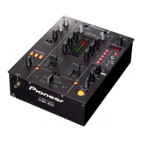
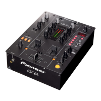
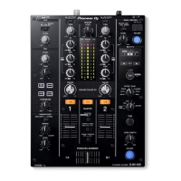
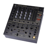
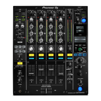
Diagram and description of the rear and front panel connectors and controls.
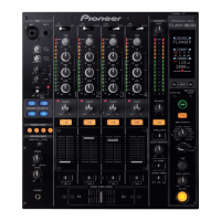
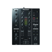
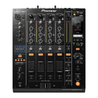
Detailed description of the front panel controls, switches, dials, and indicators.
| Channels | 2 |
|---|---|
| Weight | 3.2 kg |
| A/D, D/A Converter | 24-bit |
| Frequency Response | 20 Hz to 20 kHz |
| Total Harmonic Distortion | 0.007% or less |
| Inputs | PHONO |
| Outputs | MASTER OUT x 1, HEADPHONE MONITOR OUT x 1 |
| Effects | Delay, Echo, Flanger, Roll |
| Crossfader | Yes |
| Power Supply | AC 50/60 Hz |
| EQ | 3-band EQ per channel (-26 dB to +6 dB) |
| Signal-to-Noise Ratio | 97 dB (LINE) |