Do you have a question about the Pioneer PRO-R04U and is the answer not in the manual?
Important safety guidelines for technicians and continued customer protection, including leakage current checks.
Details on special safety characteristics of electrical components and replacement parts to prevent hazards.
Exploded view and parts list for the product's packing components.
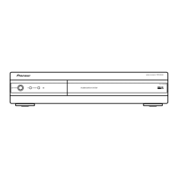
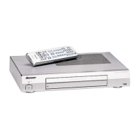
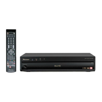
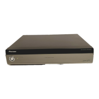
Exploded views and parts list for the external components of the unit.
Exploded views and parts list for the front panel components of the unit.
Overview of block and schematic diagrams for the Media Receiver.
Block diagram and schematic for the AV Board Assy.
Block diagram and schematic for the Power Supply Unit.
Block diagram and schematic for the DTV Tuner Board.
Overall wiring diagram illustrating connections between major assemblies.
Block diagram for the MR Main Board Assy, part 1 of 13.
Block diagram for the MR Main Board Assy, part 2 of 13.
Block diagram for the MR Main Board Assy, part 3 of 13.
Block diagram for the MR Main Board Assy, part 4 of 13.
Block diagram for the MR Main Board Assy, part 5 of 13.
Block diagram for the MR Main Board Assy, part 6 of 13.
Block diagram for the MR Main Board Assy, part 7 of 13.
Block diagram for the MR Main Board Assy, part 8 of 13.
Block diagram for the MR Main Board Assy, part 9 of 13.
Block diagram for the MR Main Board Assy, part 10 of 13.
Block diagram for the MR Main Board Assy, part 11 of 13.
Block diagram for the MR Main Board Assy, part 12 of 13.
Block diagram for the MR Main Board Assy, part 13 of 13.
Block diagram for the AV Board Assy, part 1 of 7.
Block diagram for the AV Board Assy, part 2 of 7.
Block diagram for the AV Board Assy, part 3 of 7.
Block diagram for the AV Board Assy, part 4 of 7.
Block diagram for the AV Board Assy, part 5 of 7.
Block diagram for the AV Board Assy, part 6 of 7.
Block diagram for the AV Board Assy, part 7 of 7.
Block diagram for the Bridge Assy.
Block diagram for the MDR Assy.
Block diagram for the SR Assy.
Block diagram for the Front Assy, part 1 of 2.
Block diagram for the Front Assy, part 2 of 2.
Block diagram for the LED Assy.
Block diagrams for AC SW Assy and Power Supply Unit.
Examples of waveforms for troubleshooting and analysis.
Table listing voltage measurements for various assemblies and connectors.
PCB connection diagrams for AC SW and MDR assemblies.
Instructions on how to access the service factory mode.
Conditions requiring readjustment after assembly or part replacement.
Procedure to adjust video signal levels using an oscilloscope and signal generator.
Procedure to adjust audio signal levels using a signal generator and tester.
Procedure to adjust signal levels to achieve a minimum waveform on the oscilloscope.
Troubleshooting guide for diagnosing image and sound issues.
Explains processing related to abnormal conditions in power supply and fan/temperature sensor circuits.
List and details of integrated circuits used in the unit.
| Frequency Response | 20 Hz to 20 kHz |
|---|---|
| Total Harmonic Distortion | 0.08% |
| Input Sensitivity | 200 mV |
| Channels | 2 |
| Dimensions | 420 x 133 x 365mm |