EasyManua.ls Logo

Pioneer VSX-416-S Service Manual

Pioneer VSX-416-S
19 pages
To Next Page IconTo Next Page
Page #1 background imageLoading...
Page #1 background image
ORDER NO.
PIONEER CORPORATION 4-1, Meguro 1-chome, Meguro-ku, Tokyo 153-8654, Japan
PIONEER ELECTRONICS (USA) INC. P.O. Box 1760, Long Beach, CA 90801-1760, U.S.A.
PIONEER EUROPE NV Haven 1087, Keetberglaan 1, 9120 Melsele, Belgium
PIONEER ELECTRONICS ASIACENTRE PTE. LTD. 253 Alexandra Road, #04-01, Singapore 159936
PIONEER CORPORATION 2006
RRV3377
T – ZZK MAY 2006 Printed in Japan
AUDIO/VIDEO MULTI-CHANNEL RECEIVER
VSX-416-K
VSX-416-S
CONTENTS
1. CONTRAST OF MISCELLANEOUS PARTS
........
2
2. SCHEMATIC DIAGRAM
.....................................
10
Model No. Order No. Remarks
VSX-516-K/KUCXJ RRV3329
This service manual should be used together with the following manual(s):
THIS MANUAL IS APPLICABLE TO THE FOLLOWING MODEL(S) AND TYPE(S).
For SPECIFICATIONS and PANEL FACILITIES, refer to the operating instructions.
Model Type Power Requirement Remarks
VSX-416-K MYXJ5 AC 220 V to 230 V
VSX-416-S MYXJ5 AC 220 V to 230 V
Question and Answer IconNeed help?

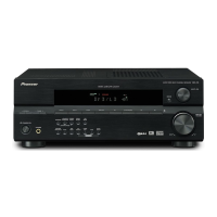
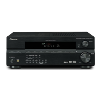
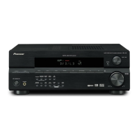
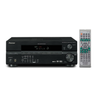
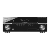
Do you have a question about the Pioneer VSX-416-S and is the answer not in the manual?

Pioneer VSX-416-S Specifications

General IconGeneral
Channels5.1
Frequency Response10 Hz - 100 kHz
Input Sensitivity200 mV
Input Impedance47 kOhm
Audio D/A Converter192 kHz / 24-bit
Built-in DecodersDolby Digital, DTS
Tuner BandsAM/FM
Preset Station Qty30
Width420 mm
Depth347 mm
Height158 mm
Tuning RangeFM: 87.5 - 108MHz
Connector TypeRCA

Summary

Pioneer Service Manual Introduction

2. SCHEMATIC DIAGRAM - Main Assembly (1/3)

Main Assembly Schematic (Part 1)

Displays the first part of the main assembly schematic diagram.

2. SCHEMATIC DIAGRAM - Main Assembly Sections

Low Pass Filter and LFE MIX Circuits

Details specific circuit blocks within the main assembly schematic.

2.2 MAIN ASSEMBLY (2/3) - Pre-Amplifier Section

Pre-Amplifier Circuitry Schematic

Provides the schematic for the pre-amplifier stage of the main assembly.

2.2 MAIN ASSEMBLY (2/3) - Control and Signal Routes

Fan Control Circuitry Schematic

Shows the schematic for the fan control system within the main assembly.

2.3 MAIN ASSEMBLY (3/3) - E2PROM and Interface

E2PROM and Microprocessor Interface Details

Details the E2PROM component and its interface with the microprocessor.

2.4 POWER PACK, TRANS2, and TRANS3 ASSYS - Overview

Power Pack Assembly Schematic Overview

Presents the overall schematic for the power pack assembly.

2.4 POWER PACK, TRANS2, and TRANS3 ASSYS - Schematics

TRANS2 Assembly Schematic Diagram

Provides the schematic diagram for the TRANS2 assembly.

TRANS3 Assembly Schematic Diagram

Provides the schematic diagram for the TRANS3 assembly.

2.5 POWER PACK ASSY (1/2) - Schematic Details

2.5 POWER PACK ASSY (1/2) - Schematic Details (Continued)

2.5 POWER PACK ASSY (1/2) - Protection and Regulation Circuits

Related product manuals