Do you have a question about the Pioneer VSX-417-S and is the answer not in the manual?
Crucial safety guidelines, warnings, and notices for technicians and users.
Step-by-step guide for performing the leakage current test.
Essential safety procedures and checks during repairs.
Procedures for adjustments, lubrication, cleaning, and shipping preparation.
Exploded view and parts list for the packing materials.
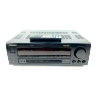
Exploded view of the receiver's external components.
Exploded view of the receiver's front panel components.
High-level functional overview of the receiver's signal paths.
Diagram showing interconnections between major assemblies.
Detailed schematic of the Main Assembly section 1.
Detailed schematic of the Main Assembly section 2.
Detailed schematic of the Main Assembly section 3.
Detailed schematic of the DSP Assembly section 1.
Detailed schematic of the DSP Assembly section 2.
Detailed schematic of the Power Pack Assembly section 1.
Detailed schematic of the Power Pack Assembly section 2.
Schematics for headphone and 5.1 channel input sections.
Schematics for display, encoder, and power key modules.
Schematics for various input/output and control circuits.
PCB layout for the Digital Input Assembly.
PCB layouts for headphone and 5.1CH input assemblies.
PCB layout for the Main Assembly.
PCB layout for the DSP Assembly.
PCB layouts for Transistor assemblies.
PCB layout for the Power Pack Assembly.
PCB layout for the Front Display Assembly.
PCB layouts for encoder and power key assemblies.
PCB layouts for Transistor and Regulator assemblies.
PCB layout for the Video Assembly.
PCB layout for the Primary Assembly.
Parts list for major assemblies and miscellaneous components.
Step-by-step analysis for DSP assembly failures.
Instructions for disassembling the unit for service.
List of ICs, their part numbers, and pin function details.
Explanations of DC, overload, and fan stop detection circuits.
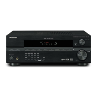
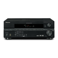
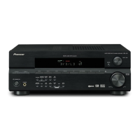
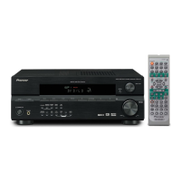
Descriptions of buttons and controls on the receiver's front panel.
Detailed explanation of remote control buttons and their functions.
Explains menu, tuner, and special function button operations.
| Channels | 5.1 |
|---|---|
| Power Output | 100 W |
| Output Power / Channel | 100 W |
| Frequency Response | 10 Hz - 100 kHz |
| Signal-to-Noise Ratio | 98 dB |
| Input Sensitivity | 200 mV |
| Input Impedance | 47 kOhms |
| Digital Sound Processor (DSP) | Yes |
| Surround Sound Effects | Dolby Digital, DTS |
| Surround System Class | 5.1 Channel |
| Tuner Bands | AM / FM |
| Preset Station Qty | 30 |
| Amplifier Type | AV |
| Output Impedance / Channel | 8 Ohm |
| Total Harmonic Distortion (THD) | 0.08% |
| Input Sensitivity/Impedance | 200 mV / 47 kOhms |
| Video Inputs/Outputs | 4 Inputs / 1 Output |
| Digital Audio Inputs | Coaxial digital input, optical digital input |
| Width | 420 mm |
| Depth | 347 mm |
| Height | 158 mm |
| Total Harmonic Distortion | 0.08% |