Rev. A 10/18
22
Application Note AN-72
www.power.com
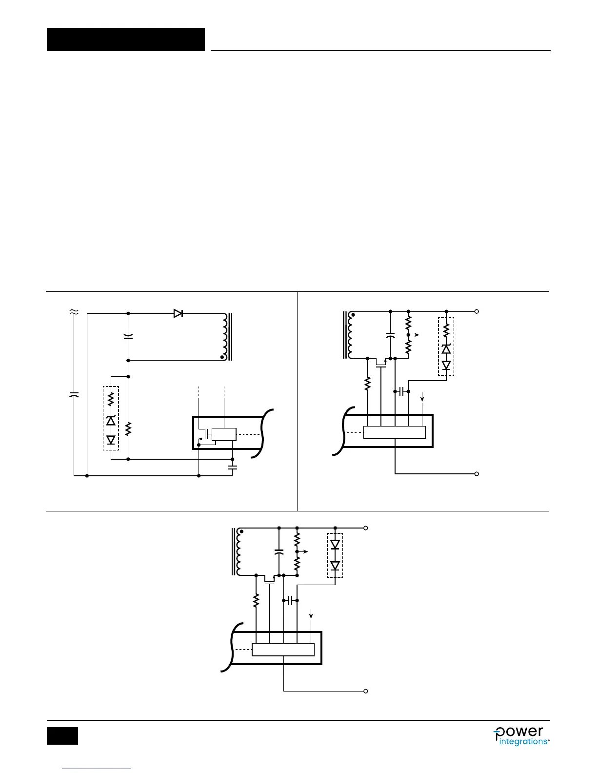
Figure 18. Output Overvoltage Protection Circuits.
a. Primary-side OVP with high current pushed into BPP via Zener V
RZ
. b. Secondary-side OVP with high current pushed into BPS via Zener V
Z
and
resistor R
Z
.
c. Secondary-side OVP with high current pushed into BPS via two diodes (for 5 V output only).
Key Applications Design Considerations
Output Power Table
The output power table in the data sheet (Table 1) represents the
maximum practical continuous output power that can be obtained
under the following conditions:
1. The minimum DC input voltage is 90 V or higher for 85 VAC input,
220 V or higher for 230 VAC input (or 115 VAC with a voltage-
doubler). Input capacitor voltage should be sized to meet these
criteria for AC input designs.
2. Efciency assumptions depend on power level. Smallest device
power level assumes efciency >84% increasing to >89% for the
largest device and are quite conservative.
3. Transformer primary inductance tolerance of ±10%.
4. Reected output voltage (V
OR
) is set to maintain K
P
= 0.8 at
minimum input voltage for universal line and K
P
= 1 for high-line
designs.
5. Maximum conduction loss for adapters is limited to 0.6 W, 0.8 W
for open frame designs.
6. Increased current limit is selected for peak and open frame power
designs and standard current limit for adapter designs.
7. The part is board mounted with SOURCE pins soldered to a
sufcient area of copper and/or a heat sink to keep the SOURCE
pin temperature at or below 110 °C.
8. Ambient temperature of 50 °C for open frame designs and 40 °C
for sealed adapters is assured.
9. To prevent reduced power delivery, due to premature termination
of switching cycles, a transient K
P
limit of ≥0.5 is used. This
prevents the initial current limit (I
INT
) from being exceeded at
MOSFET turn-ON.
10. It is unique feature in InnoSwitch3 that a designer can set the
operating switching frequency between 25 kHz to 95 kHz depending
on the transformer design. One of the ways to effectively lower
device temperature is to design the transformer to operate at low
switching frequency, a good starting point is 60 kHz for larger
device such as size 8, but for smaller device such size 2, 80 kHz is
appropriate.
Primary-Side Overvoltage Protection
Primary-side output overvoltage protection provided by the InnoSwitch3 IC
uses an internal latch that is triggered by a threshold current of I
SD
owing into the PRIMARY BYPASS pin. For the bypass capacitor to be
effective as a high frequency lter, the capacitor should be located as
PI-8481-101017
Primary FET
and Controller
+V
BULK
C
BIAS
C
IN
N
B
D
BIAS
D V
S
BPP
InnoSwitch3
R
Z
D
B
R
BP
V
RZ
Secondary
Control IC
IS
V
OUT
RTN
BPS
FB
FB
GND
SR
FWD
InnoSwitch3
Diode
OVP
C
BPS
PI-8476-101017
IS
V
OUT
RTN
BPS
FB
GND
SR
FWD
R
Z
V
Z
= (V
OUT
× 1.25) –
(4 × 4 – V
BPS
)
V
Z
C
BPS
Zener
OVP
Secondary
Control IC
InnoSwitch3
FB
D
B