30 31
ORDER
32
31
11
V
13
I +
A
V
A
5225
50050
12
V +
JP 2JP 1
43
41
22
21
24
23
42
f in
S0
NPN
Vreg.
JP 4
JP 3
13k3
3k48
D/A
Option
Supply gnd.
Gnd.
I + V
Out
I
Out
V
Out
0…20
mA
Input +
+ 24 VDC
Input gnd.
5…17 VDC
Error
Relay 1 / NPN
Relay 1 / dig. gnd.
Front comm.
5…17V+
NamurTacho
Dig out 2
Dig out 1
Relay 2
Relay 2 / PNP
Supply +24 VDC
Spec.
V Out
NPN pull up:
6.7 mA: JP4 ON
1.7 mA: JP3 ON
Sup.
+
Sup.
+
NPNPNP Contact
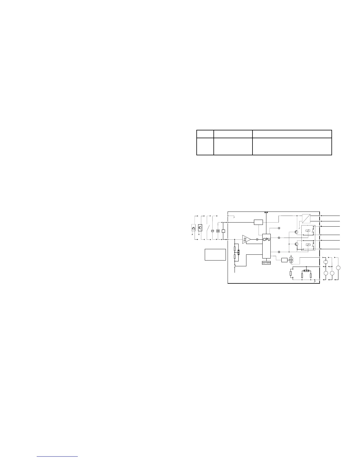
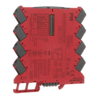
BLOCK DIAGRAM
Frequency generator:
Min. period ................................................ 50 µs
Max. frequency ........................................... 20 kHz
Duty cycle ................................................... 50%
Relay output:
Isolation, test / operation ........................... 3.75 kVAC / 250 VAC
Frequency max. .......................................... 20 Hz
V
max.
......................................................... 250 VRMS
I
max.
........................................................... 2 A / AC
Max. AC power ......................................... 500 VA
Max. load at 24 VDC .................................. 1 A
GOST R approval:
VNIIM, Cert. no. .......................................... See www.prelectronics.com
Observed authority requirements: Standard:
EMC 2004/108/EC ..................................... EN 61326-1
LVD 2006/95/EC ......................................... EN 61010-1
PELV/SELV .................................................. IEC 364-4-41 and EN 60742
Of span = Of the presently selected range
Type Version Output
5225 Standard : A Analogue + NPN / PNP
Analogue + relay output
: 1
: 2