11
4TOLB-3L1
1306, Issue 2, May 1992
the card-edge connector pins and pc board switches. The alignment procedures and test
equipment setups are shown in Figure 7. A brief description of the TEST jack and adapter
is given below.
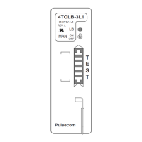
1) TEST Jack—The MAC jack (J1) on the front panel of the unit permits the insertion of
a test card for alignment and measurement of circuit parameters. Additional
information on the MAC jack is given in section 6, Maintenance.
2) Adapter—The MAC jack to bantam jack adapter provides bantam jack access to
the test points available through the MAC jack on the front panel of the channel unit.
The adapter can be the Pulsecom B105097 MAC jack to bantam jack adapter or
equivalent. A detailed description of the B105097 is provided in Pulsecom Practice
Section 1303.
4. CIRCUIT DESCRIPTION
A. VF Transmit Operation
The following paragraphs describe the operation of the channel unit as shown in Figure 8,
Functional Diagram. VF signals enter the channel unit through the transmit input port
(T and R leads), where a transformer provides DC isolation and maintains the required
600-ohm impedance.
The signals then are coupled through the transmit amplifier to the attenuator circuit, which
provides from 0 to 32.5 dB of attenuation in 0.1-dB steps. The attenuation switches are
selected to obtain the required transmission level (–8.5 TLP) at the transmit path TEST
jack (J1-1/7). The VF signals are filtered and routed to the transmit sampling gate.
The common equipment, which handles 8000 frames of information per second, causes
the transmit sampling gate to close during the proper channel in each frame. At the proper
channel time, when the TWD, TSP(N), and TSQ(N) leads are all at logic one, the control
lead to the transmit sampling gate switches to logic zero to allow the common equipment,
through the transmit output port (leads TPAM and TPAMG), to sample and encode the
voice signal at that instant.
The TNEN output is at logic zero when the transmit input control leads, TSP(N) and
TSQ(N), are both at logic one. This output indicates to the D4 common equipment
transmit unit that the selected voice-type channel unit is installed in the channel bank.
The TEST jack (J1), accessible from the front panel, allows access to the transmit voice
path for test purposes. A test card inserted into the J1 jack provides access to the output of
the attenuator (terminal J1-1) and the input of the transmit filter (terminal J1-7).