LTE Standard Module Series
EM05-G Hardware Design
EM05-G_Hardware_Design 27 / 69
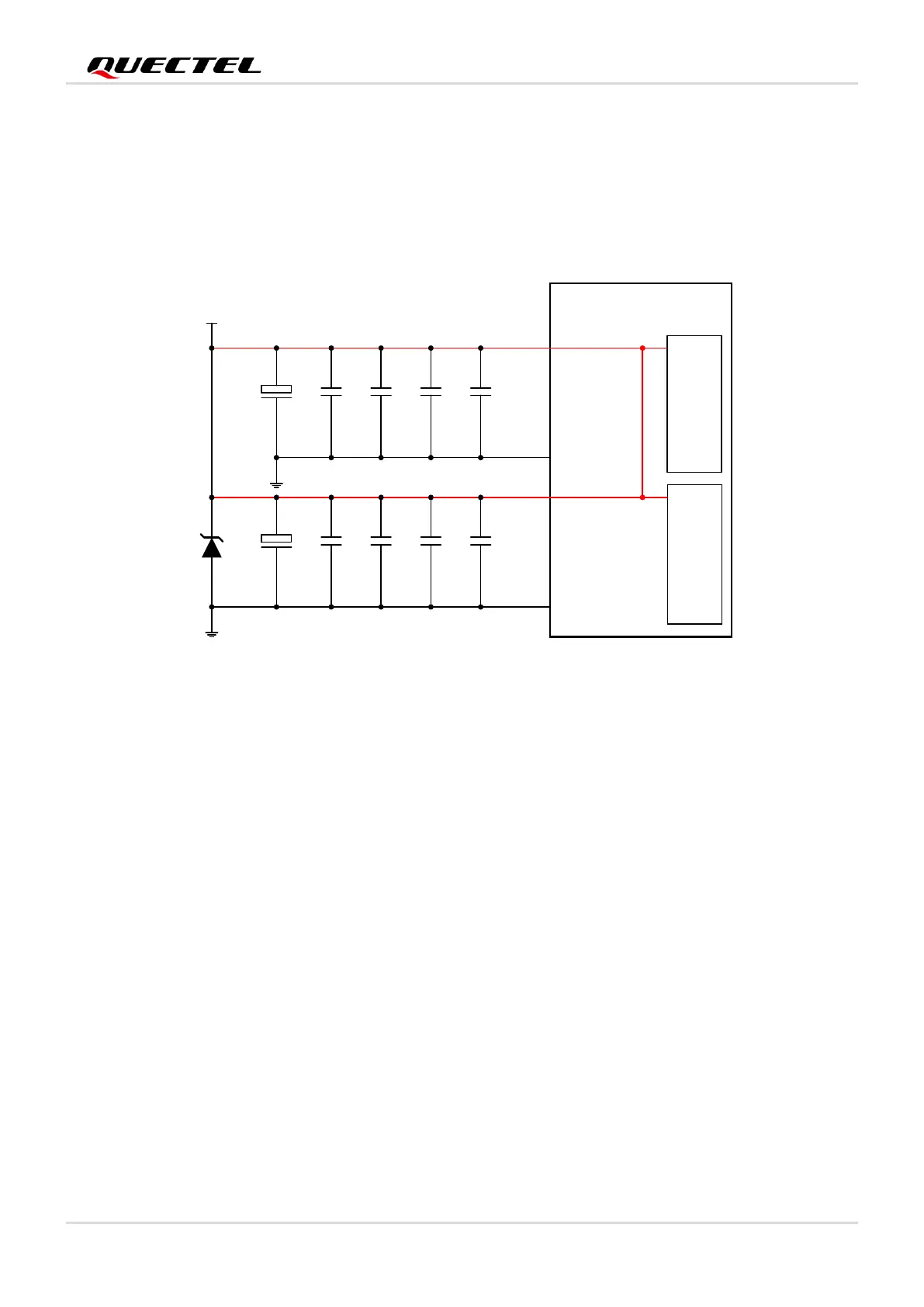
composing the MLCC array, and place these capacitors close to VCC pins. The width of VCC trace
should be no less than 2.5 mm. In principle, the longer the VCC trace is, the wider it should be.
In addition, to guarantee stability of the power supply, use a zener diode with a reverse zener voltage of
5.1 V and a dissipation power of higher than 0.5 W. The following figure shows a reference circuit for the
VCC.
Figure 7: Reference Circuit for the VCC
3.3.2. Reference Design for Power Supply
Power design is important for the module, as the performance of the module largely depends on the
power source. The power supply of the module should be able to provide a sufficient current of 2.0 A at
least. If the voltage drop between the input and output is not too high, it is suggested that an LDO should
be used to supply power for the module. If there is a big voltage difference between the input source and
the desired output (VCC = 3.3 V Typ.), a buck converter is preferred to be used as the power supply.
The following figure shows a reference design for +5 V input power source. The typical output of the
power supply is about 3.3 V and the maximum load current is 2.0 A.