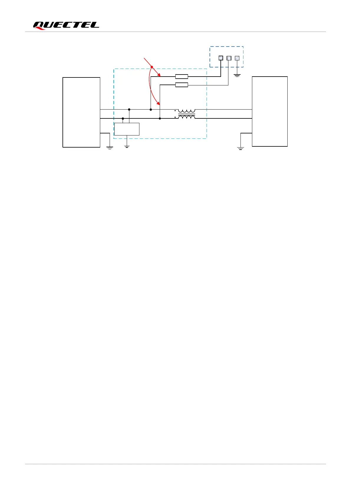
Figure 18: Reference Circuit of USB 2.0 Interface
A common mode choke L1 is recommended to be added in series between the module and customer’s
MCU to suppress EMI spurious transmission. Meanwhile, the 0 Ω resistors (R3 and R4) should be added
in series between the module and the test points to facilitate debugging, and the resistors are not
mounted by default. To ensure the integrity of USB data line signal, L1, R3 and R4 components must be
placed close to the module, and also these resistors should be placed close to each other. The extra
stubs of trace must be as short as possible.
To meet USB 2.0 specification, the following principles should be complied with when designing the USB
interface.
⚫ Route the USB signal traces as differential pairs with ground surrounded. The impedance of USB
differential trace is 90 Ω.
⚫ Do not route signal traces under crystals, oscillators, magnetic devices, PCIe and RF signal traces.
Route the USB differential traces in inner-layer of the PCB, and surround the traces with ground on
that layer and with ground planes above and below.
⚫ Pay attention to the influence of junction capacitance of ESD protection components on USB data
lines. Typically, the capacitance value should be less than 2 pF.
⚫ Keep the ESD protection components as close to the USB connector as possible.