find MEM* on
the
big Schematic, you will
notice
it
controls
the
ROM!RAM buffers.
The
outputs
of
the
buffers are tied
to
the
data
bus.
We
now
get
ROM
data
onto
the
data
bus. Has it
got
a way
to
get
to
the
CPU? Yes, it does.
Reme.mber
that
RD
is
low because
the
CPU
is
in
a Memory Read cycle. Since
this
is
so, DBIN*
is
low and OBOUT*
is
high.
The
low
at
OBIN*
enables
the
CPU's
input
data
buffers and
ROM
data
is
available
for
the
CPU.
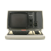
Keyboard
Decoding
The
Keyboard
is
located from address 3800
to
38FF.
The
Keyboard
is
memory,
so RAS* will
be low. A
15
is
low because we are generating
address
codes
under
8000.
Looking
at
our
binary location
for
the
Keyboard, we find A
14
low,
A13
and
A12
high. With this
input
combi-
nation,
Z21 will be active
and
pin 12 will be iow
(Output
3). Pin 12
is
tied
to
Z36, pin 4. Accord-
ing
to
the
breakdown,
A
11
is
high.
Z37,
pin 4,
outputs
a low
to
Z36, pin 5.
The
"incorrectly
drawn"
OR gate tells us we need
both
inputs
low
for
a low
output.
We've
got
it, so pin 6
of
Z36
is
also low. Pin 6
of
Z36
is
tied
to
pins 12
and
10
of
Z36. Checki
ng
on
the
status
of
A10,
we find it listed as being low during a Keyboard
address
output.
Since
Z36,
pins 12 and 13 are
low, we'll get a low
at
pin 11. KYBD*
is
gener-
ated
at
this
pin.
Finding KYBO* on
the
big Schematic, you'll see
it
goes
to
the
enable
inputs
of
the
data
buffers
for
the
Keyboard.
The
lower
order
address lines
are tied
to
one
end
of
the
keyboard
matrix,
while
the
other
end
of
the
matrix
is
tied
to
the
data
bus,
through
the
buffers. If a key
is
pressed,
an address line will be
"shorted"
to
a
data
line.
Assume
for
now
that
this
scheme works. We'll
analyze
the
Keyboard later.
The
DBOUT*
and
DBIN* signals are switched
the
same way as if
we had a
ROM
select. Therefore, Keyboard data
will get
to
the
CPU's
data
bus
for
processing.
22
Video Display RAM Select
In
the
binary
breakdown
for
the
Memory Map,
you will notice
that
the
binary
out
for
the
Video
RAM
address
is
almost
the
same as
the
Keyboard
except
for
bit
A10.
Z21,
pin
12,
will
output
a
low
to
Z36,
pin
4.
Since A11
is
still high,
Z37,
pin 4 will supply a low
to
pin 5
of
236.
There-
fore, pin 6
of
236
is
low,
just
as if a keyboard
was selected. Since A
10
is
now
high, Z36, pin
11
is
high and KYBD*
is
not
active.
But
Z36,
pin
10
is
low and so
is
pin 9 (due
to
the
effects
of
inverter
Z52,
pins 1 and 2\. Thus, Z36,
pin
8 goes low and we have caused VID*,
the
Video
RAM
select,
to
become active. Assume for
now
that
VI
D*
does
select
the
Video
RAMS.
We'll
discuss
what
it
does and
how
it does it later.
4K
RAM
Decoder
As shown
on
the
Memory Map,
the
addresses
which select
RAM
extend
from
hex
4000
to
4F
FF
for
4K.
The
binary
breakdown
lists
the
state
of
A15
as a 0.
A14
is
high, and
A13
and
A12 are low.
We
are accessing
memory,
so RAS*
is
low. Hence,
Z21
will be active and
output
4
will
be
low (pin 7). DIP
shunt
Z3
passes
this
low
through
pins 2 and
15,
and
it
is
applied
to
Z74,
pin
10.
It also
is
outputted
by
the
decoder
section as RAM*. RAM* will select
the
CE
on
all
of
the
RAMs,
after
it passes
through
DIP
shunt
271.
(It's
shown
on
sheet
2
of
the
large
Schematic,)
The
selection
of
the
data
bus for RAMs
is
handled
the
same way during a ROM-Read
operation.
MEM* will go low because RD*
went
low.
But
during a CPU
data
dump
from CPU
to
RAM, MEM* does
not
select
the
data
bus
buffers for
the
RAM. Instead
of
RD* being
active, WR*
is
low.
We
don't
need
the
RaMI
RAM
buffers
because
the
RAM
data
inputs
are
on
the
output
side
of
the
buffers. Only during a
ROM/RAM
read
operation
do
we
need
M~M*.
 Loading...