Renesas VUI Reference Solution VOICE-RA2L1 Engineering Manual
VOICE-RA2L1 Engineering Manual Rev.1.0 Page
of 14
June 2022
8.5 Debug
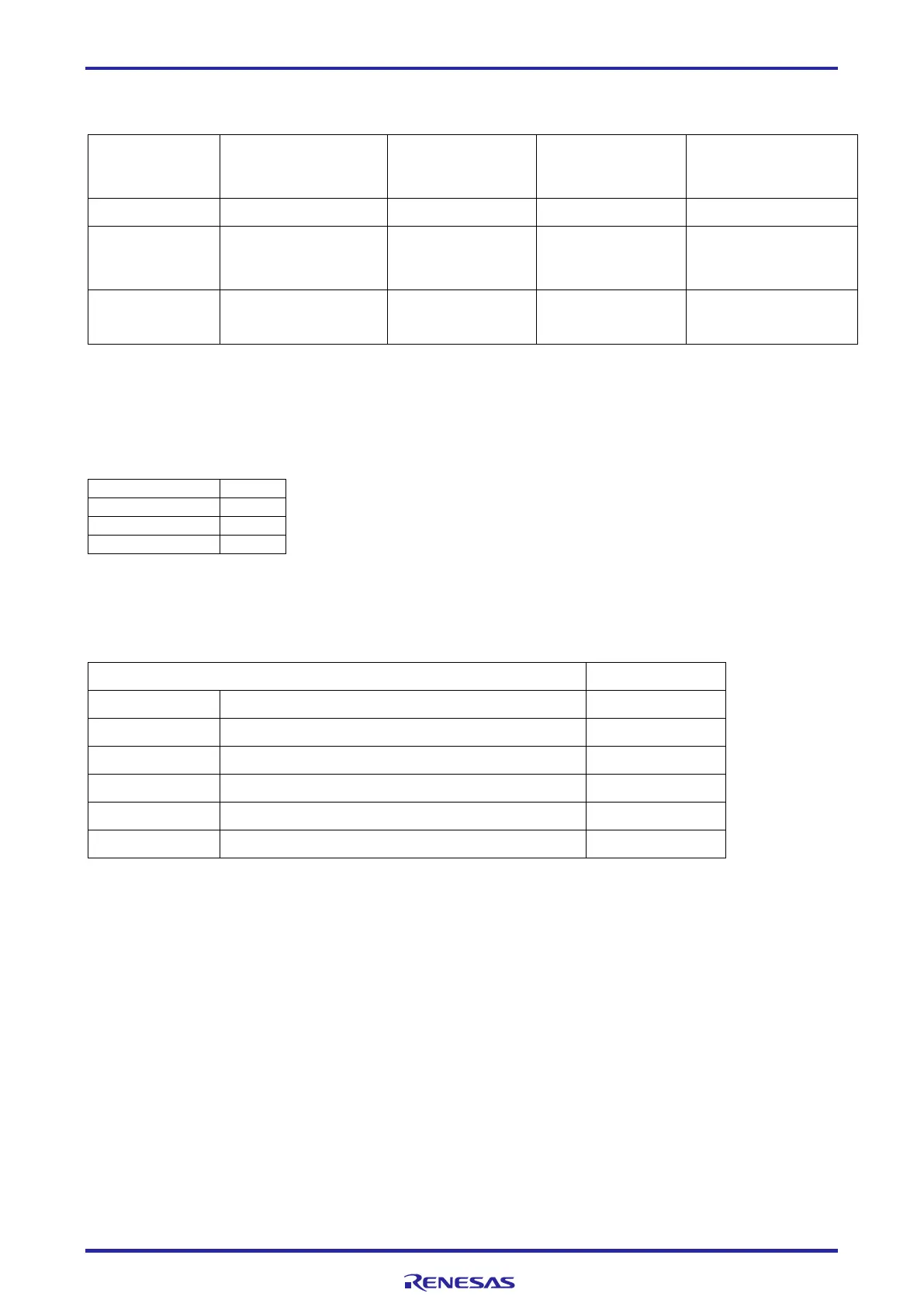
The VOICE-RA2L1 board supports following three debug modes.
Debug MCU
(one that connects
to the IDE on PC)
Target MCU
(one that is being
debugged)
Debugging
Interface/Protocol
20-pin connector (J9)
or 10-pin connector
(J8)
20-pin connector (J9)
or 10-pin connector
(J8)
Notes:
• Please cut E9 for Debug out function
• See Table 14 for the Debug USB connector pin definition.
• See Table 15 for the 10-pin JTAG connector pin definition.
• See Table 16 for the 20-pin JTAG connector pin definition.
Table 11. Jumper Connection Summary for Different Debug
The J-Link On-Board (JLOB) debug interface supporting JTAG, SWD debug interface and also supports the
VCOM (Virtual COM port) function. The debug MCU is a Renesas RA4M2, programmed with J-Link firmware
licensed by Segger. This interface includes one USB micro-B connector (J6) for host debug through the J-
Link MCU, one 10-pin and one 20-pin debug header (supporting JTAG and SWD).
Table 12. Debug USB Connector
USB ID, jack internal switch, cable inserted
 Loading...


