Home
RF-Star
Computer Hardware
RF-43UP
Page 33 (Optional Packaging)
RF-Star RF-43UP - Optional Packaging; Figure 14. Recommended Reflow for Lead Free Solder; Figure 15. Optional Packaging Mode
35 pages
Manual
Save Page as PDF
To Next Page
To Next Page
To Previous Page
To Previous Page
Loading...
RF
-43UP
www
.szrfstar
.com
V1.3 - Jan., 2020
Shenzhen
RF
-sta
r T
echnology C
o., Ltd.
Page
32
of
34
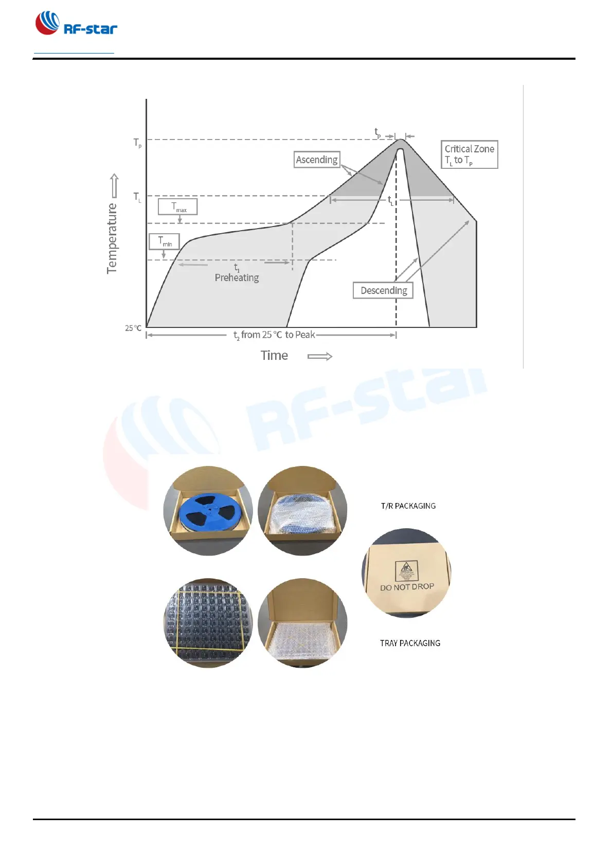
Figure
14
. Recommended
Reflow for Lead Free Solder
8.5
Optional Packaging
Figure
15
. Optional Packaging Mode
Note: Default tray packaging.
32
34
Table of Contents
Main Page
Default Chapter
2
RF-Star Lora Module List
2
1 Device Overview
3
Description
3
Key Features
3
Applications
3
Functional Block Diagram
4
Part Number Conventions
4
Figure 1. Functional Block Diagram of RF-43UP
4
Figure 2. Part Number Conventions of RF-43UP
4
Table of Contents
5
Table of Figures
6
Table of Tables
7
2 Module Configuration and Functions
8
Module Parameters
8
Table 1. Parameters of RF-43UP
8
Module Pin Diagram
9
Pin Functions
9
Figure 3. Pin Diagram of RF-43UP
9
Table 2. Pin Functions of RF-43UP
9
3 Specifications
11
Recommended Operating Conditions
11
Handling Ratings
11
Current Consumption
11
Table 3. Recommended Operating Conditions of RF-43UP
11
Table 4. Handling Ratings of RF-43UP
11
Table 5. Current Consumption of RF-43UP
11
4 Application and Layout
13
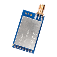
Module Photos
13
Recommended PCB Footprint
13
Figure 4. Photos of RF-43UP
13
Figure 5. Recommended PCB Footprint of RF-43UP (MM)
13
Schematic Diagram
14
Reference Design of the Connection between MCU and Module
14
Figure 6. Schematic Diagram of RF-43UP
14
Figure 7. Reference Design of the Connection between MCU and Module
14
5 Module Functions
15
Working Mode
15
Mode Switching (0 for Low Level, 1 for High Level)
15
Normal Mode
16
Wake-Up Mode
17
Low-Power Mode
17
Sleep Mode
17
Data Security
18
6 Module Functions
19
Transparent Transmission
19
Fixed Point Transmission
19
Figure 8. Transparent Transmission Function Diagram
19
Broadcast and Listening
20
Module Reset
20
Figure 9. Point Transmission Function Diagram
20
Function
21
Figure 10. en Timing Diagram of Wake-Up Sleep MCU
21
Figure 11. en Timing Diagram During Sending Data
21
Figure 12. en Timing Diagram During Receiving Data
22
Figure 13. en Timing Diagram During Setting Data
22
7 Command Format
23
AT Command
23
Parameters of Command Setting
24
Format
24
Detailed Parameters
24
Examples
27
8 Implementation
30
Hardware Design
30
Trouble Shooting
31
Unsatisfactory Transmission Distance
31
Vulnerable Module
31
High Bit Error Rate
31
Electrostatics Discharge Warnings
31
Soldering and Reflow Condition
32
Table 6. Temperature Table of Soldering and Reflow
32
Optional Packaging
33
Figure 14. Recommended Reflow for Lead Free Solder
33
Figure 15. Optional Packaging Mode
33
9 Revision History
34
10 Contact Us
35
Related product manuals
RF-Star RF-BM-BG22A3
27 pages
RF-Star RF-BM-BG22Ax Series
23 pages